SOLIDWORKS Thermal Stress From Beginning to End
Table of Contents
When our products experience thermal loading, it introduces stresses that we must understand for the sake of function and safety. The SOLIDWORKS Simulation portfolio offers several FEA tools at different price points for different thermal situations. This article will review them, so you can determine the best solution for your needs.
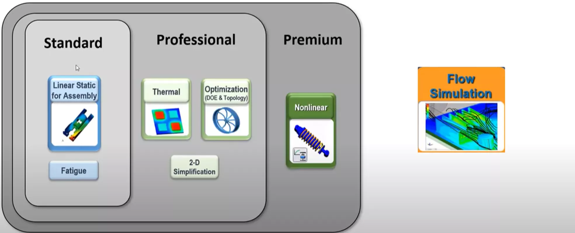
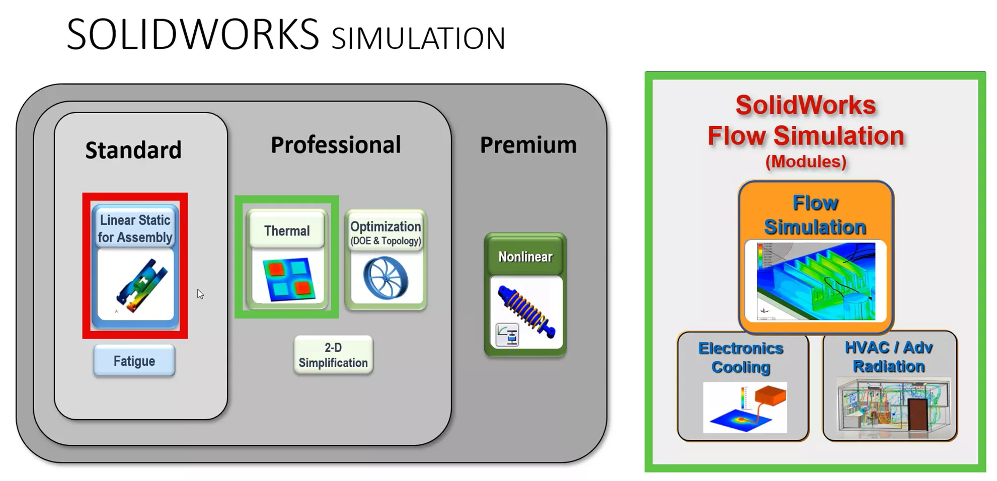
When it comes to obtaining thermal stress results with the SOLIDWORKS Simulation portfolio, the following software solutions are available: linear static studies under SOLIDWORKS Simulation Standard and nonlinear studies with SOLIDWORKS Simulation Premium.
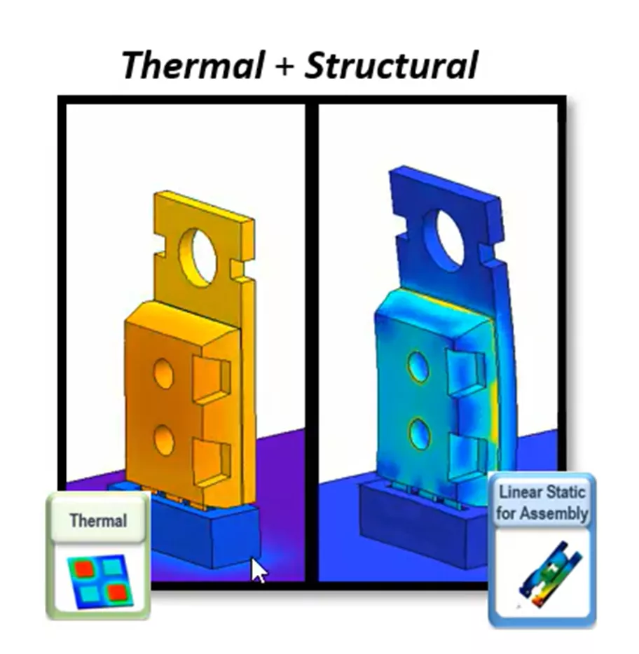
For the workflow explored in this article, SOLIDWORKS Premium will be our main vehicle for obtaining stress results. First, we'll obtain thermal results from a thermal study using Simulation Professional or SOLIDWORKS Flow Simulation, then bring these thermal results into a structural study to obtain the final thermal stress results.
Where Do Thermal Stresses Come From?
There are two primary scenarios where thermal stresses are generated. The first scenario is stress generated from the bonding among components with different thermal expansion coefficients. Below are two blocks that have been bonded side by side and thermally loaded with two different thermal expansion coefficients.
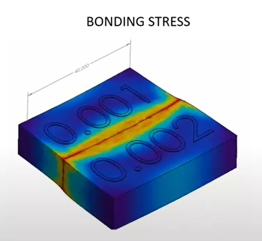
Notice that the block labeled 0.002 has a thermal expansion that is larger, so it expands by more. The thermal stress is being generated due to the difference in expansion among the bonded surfaces. The bonded face with the smaller coefficient is put in tension, while the bonded face with the larger coefficient is put in compression. We can see in red where the bonding stresses are developing.
The second scenario causing thermal stress is anywhere there is non-uniform temperature development.
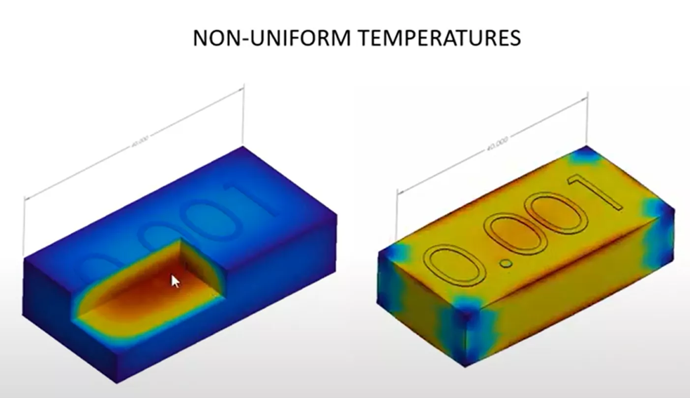
We can see a cutaway of the block above on the left, where a thermal load was applied. The thermal load is showing that it is primarily hot in the center and cooler on the outside. The response of the geometry due to this thermal loading and the thermal expansion coefficient is a ballooning expansion of the geometry, primarily from the inside, causing the stresses seen on the right of the above graphic.
Exploring Thermal Stresses
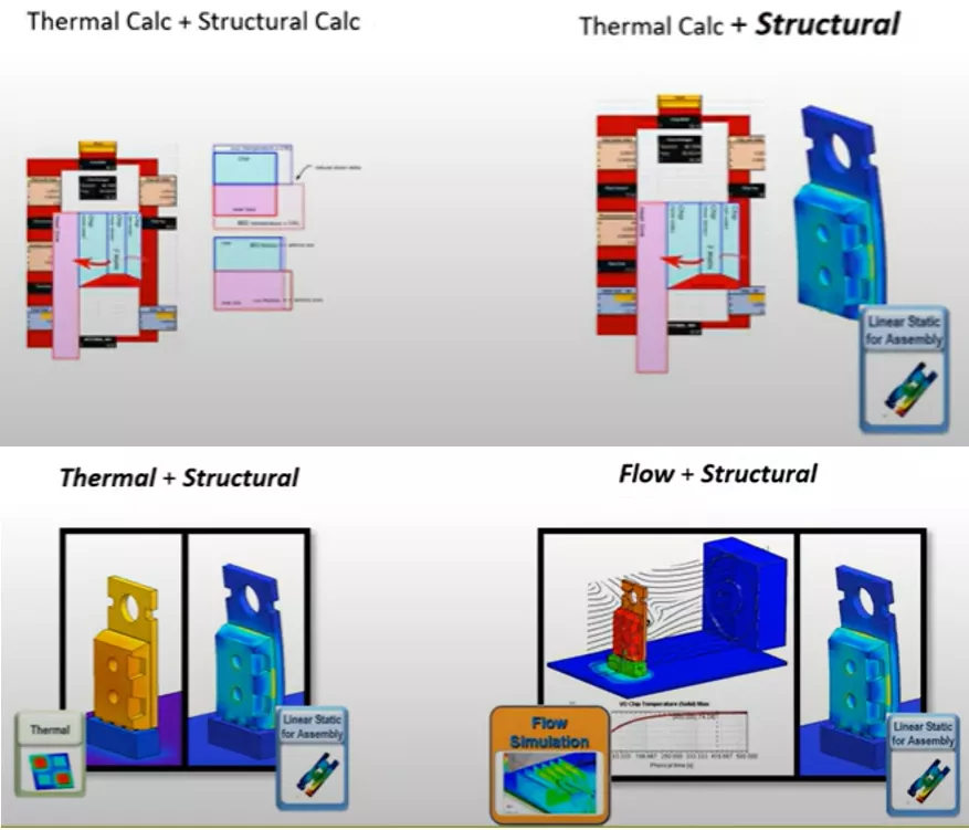
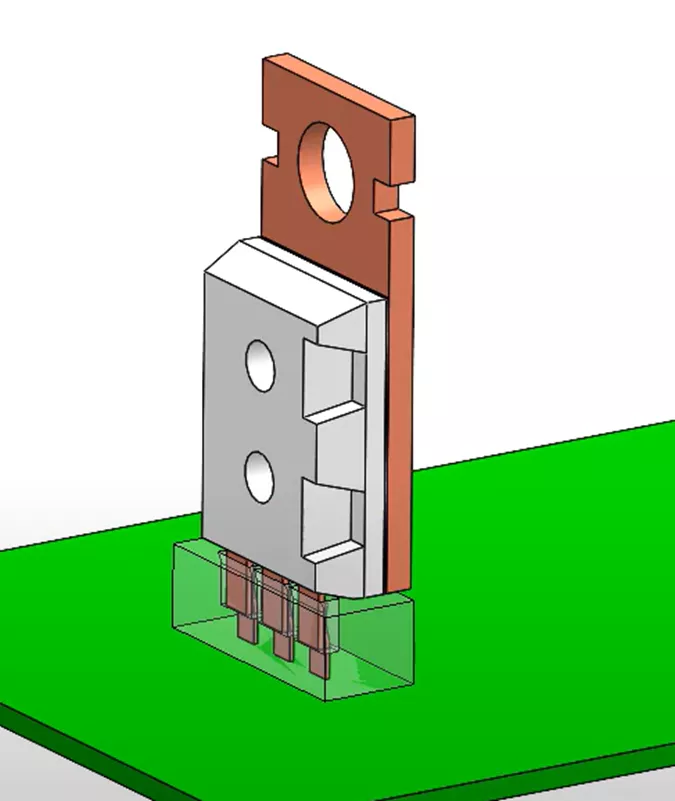
We will review several ways to explore thermal stress results, starting with simple methods using hand calculations, and ending with more advanced simulation calculations using fluid dynamics. This exploration will center around a simple microphip (depicted below).
We have a fan blowing over a ceramic microchip that is generating about 3 watts of heat. That heat will dissipate to the surrounding air. The goal is to determine the thermal stress that develops around the contact region between the microchip and the heat sink.
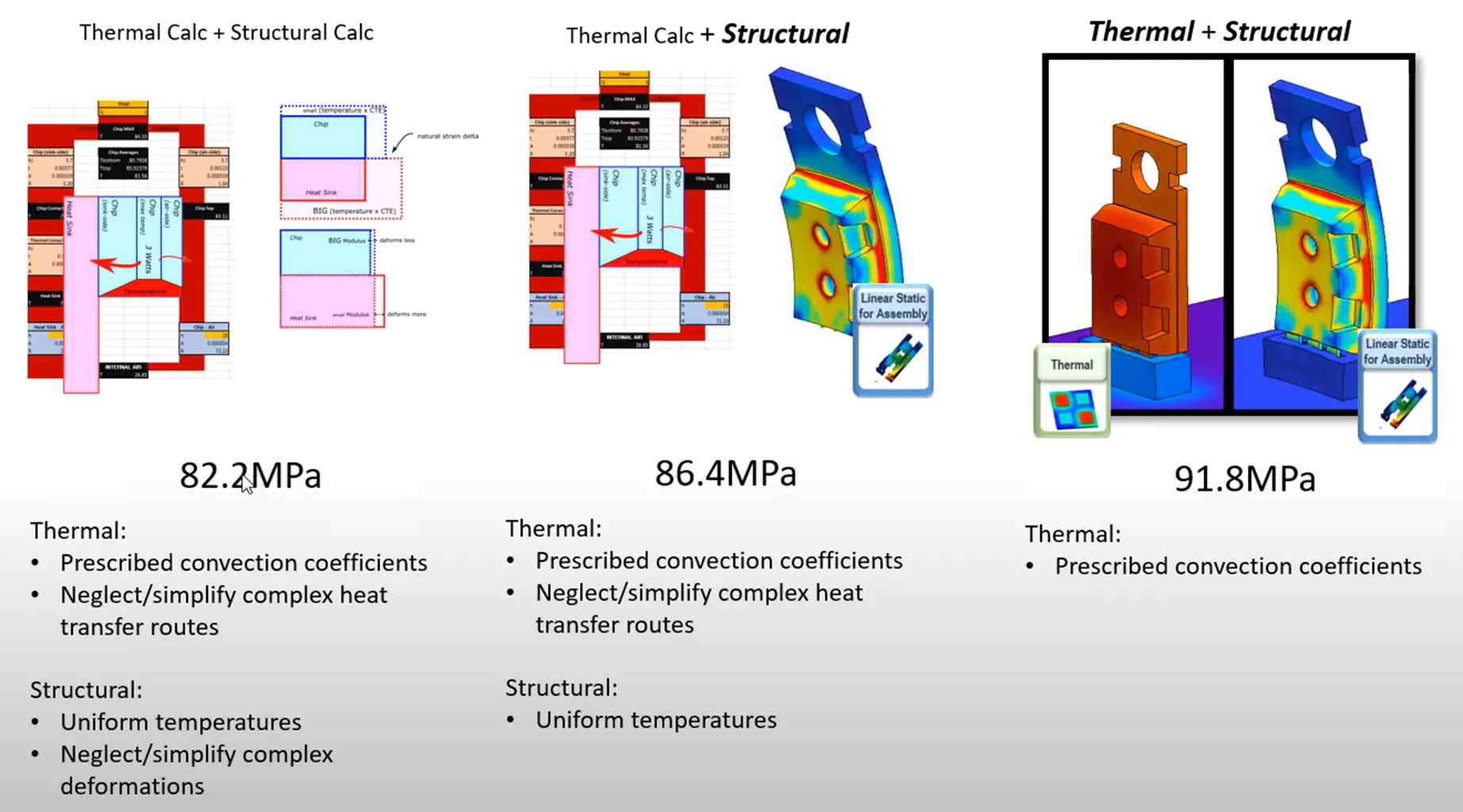
Determining The Thermal Stress in Two Steps
For this type of study, we will need two steps. First, we will calculate the heat transfer and equilibrium temperature distribution. Then we will take those temperatures and plug them into a structural study to calculate the stresses.
Method 1
Calculating Thermal Stress Exclusively Using Hand Calculations
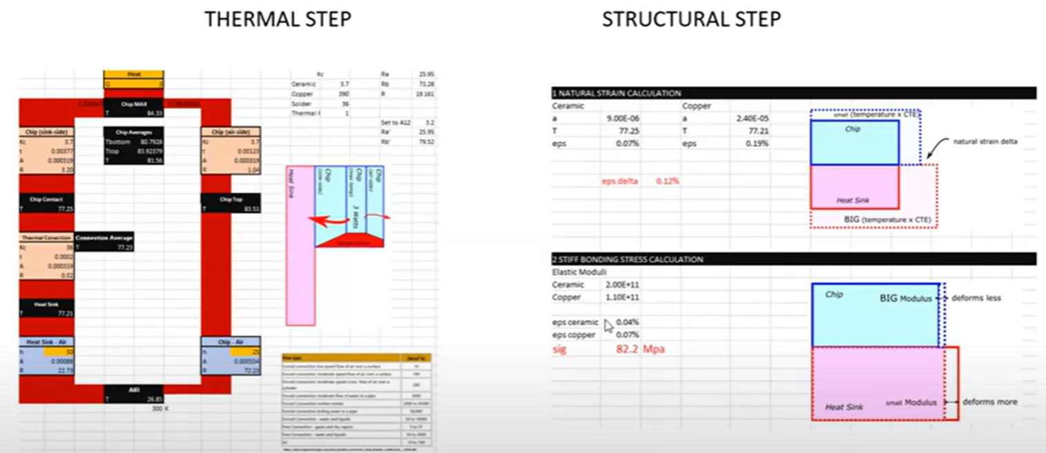
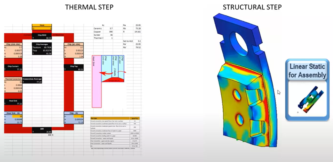
Let's begin by exploring the thermal stress of our model with a simple hand calculation. The two-step workflow is depicted below and has been set up with some hand calculations.
- Download the spreadsheet used for the hand calculations for reference.
Below is one of the major assumptions we are making in our hand calculations.
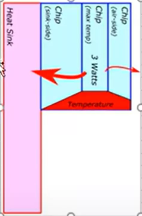
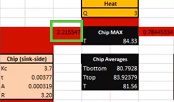
The larger red arrow shows that most of the 3-watt heat energy and heat transfer will happen from the microchip to the heatsink to get the surrounding air. Heat energy sees the lowest thermal resistance if it travels in that direction. A smaller magnitude of heat energy, depicted by the smaller red arrow to the right, will also go directly to the air via the microchip.
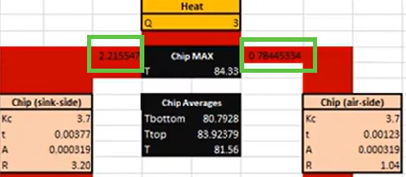
In the above section of the hand calculation, notice that most of the heat energy, about 2.2 watts, or 3/4ths of it, goes to the left to the heatsink geometry, and about 1/4th of it goes to the right and directly to the surrounding air.
Another major assumption we must make for this calculation is to decide how effective it is to transfer the generated heat of 3 watts to the air. In other words, what should the convection coefficient be for the pathway from the heatsink to the air and directly from the microchip to the air? This is depicted with the orange cells in the next portion of the calculation.
For general situations, you can find tables online with recommended convection coefficients (such as this one below):
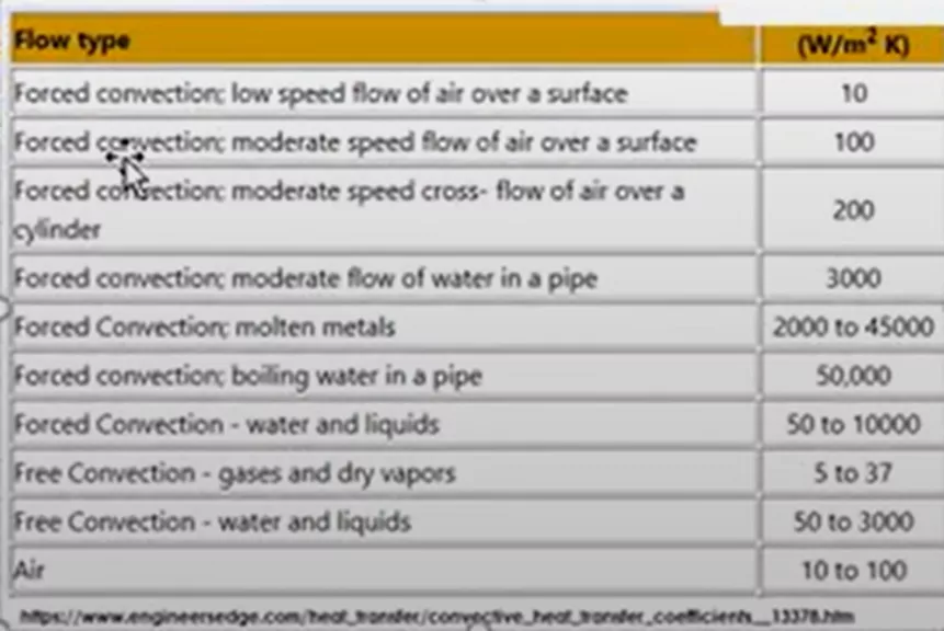
The first two line items on this table are the closest to our flow type, so we must decide where our specific thermal scenario lies along that trend line between 10 and 100 W/m2K. This decision makes a big difference in the results and must be chosen carefully.
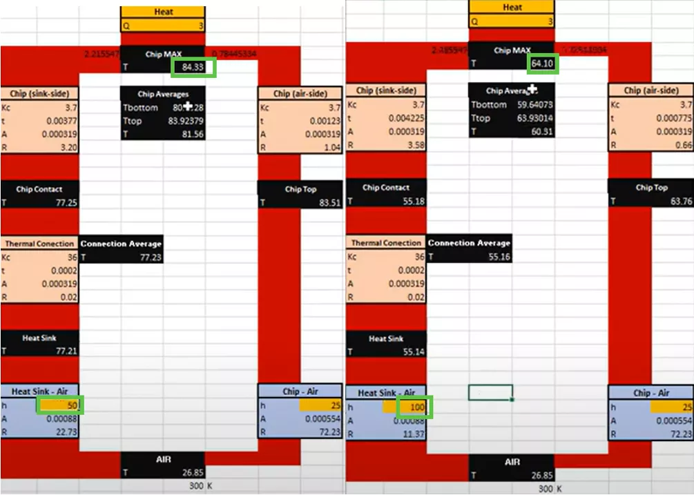
If a coefficient of 50 is used, the chip heats up to 84.3°C. If a coefficient of 100 is entered, the chip temperature drops significantly to 64.1°C. We will keep 50 for this example.

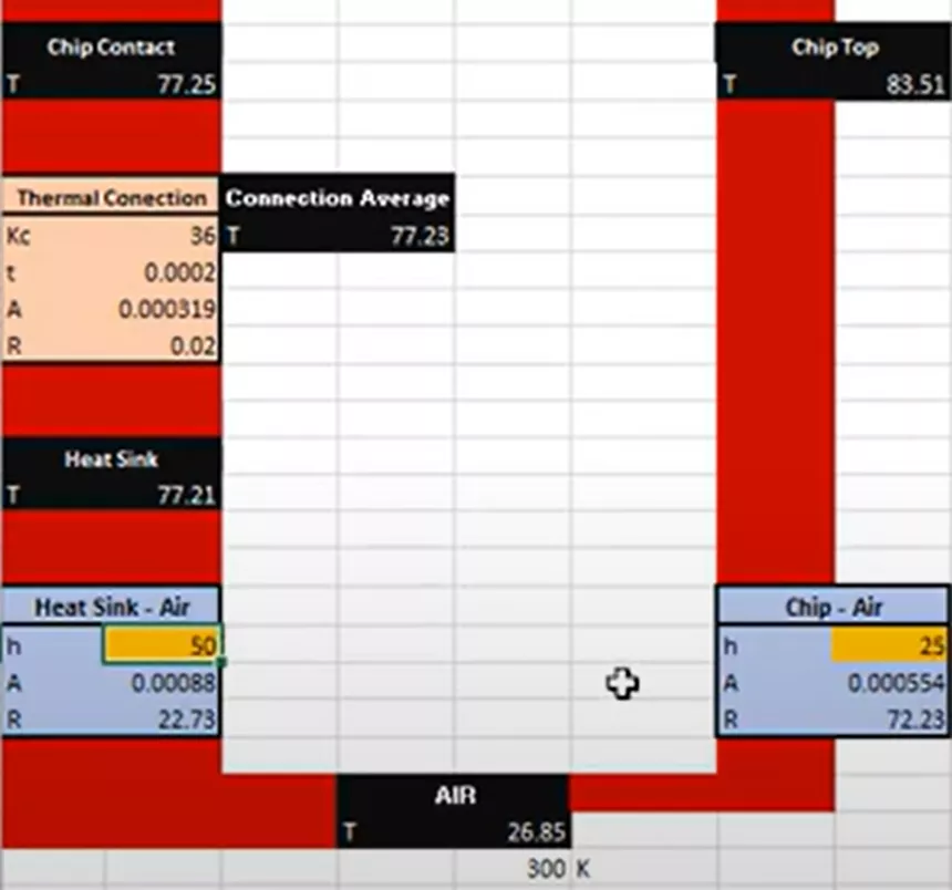
Now, we'll take the summarized temperature results and incorporate them into the structural hand calculation step shown below.
On the structural side, we need to account for how the two bodies expand when thermally loaded.
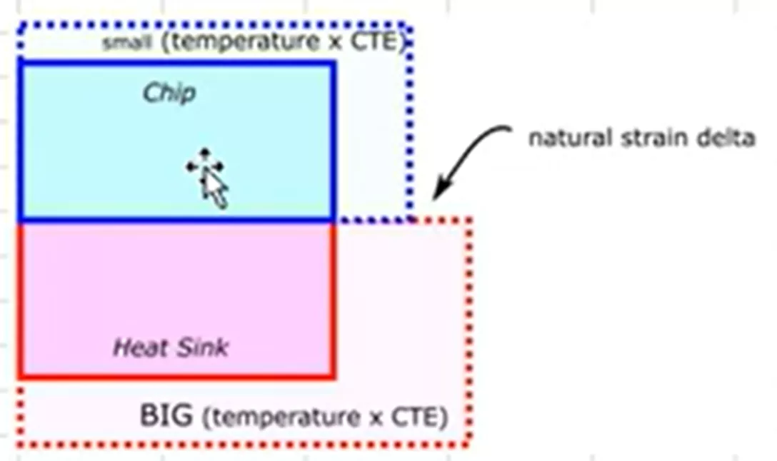
As mentioned earlier, when bodies are connected or bonded together, this is when you will see stresses begin to develop.
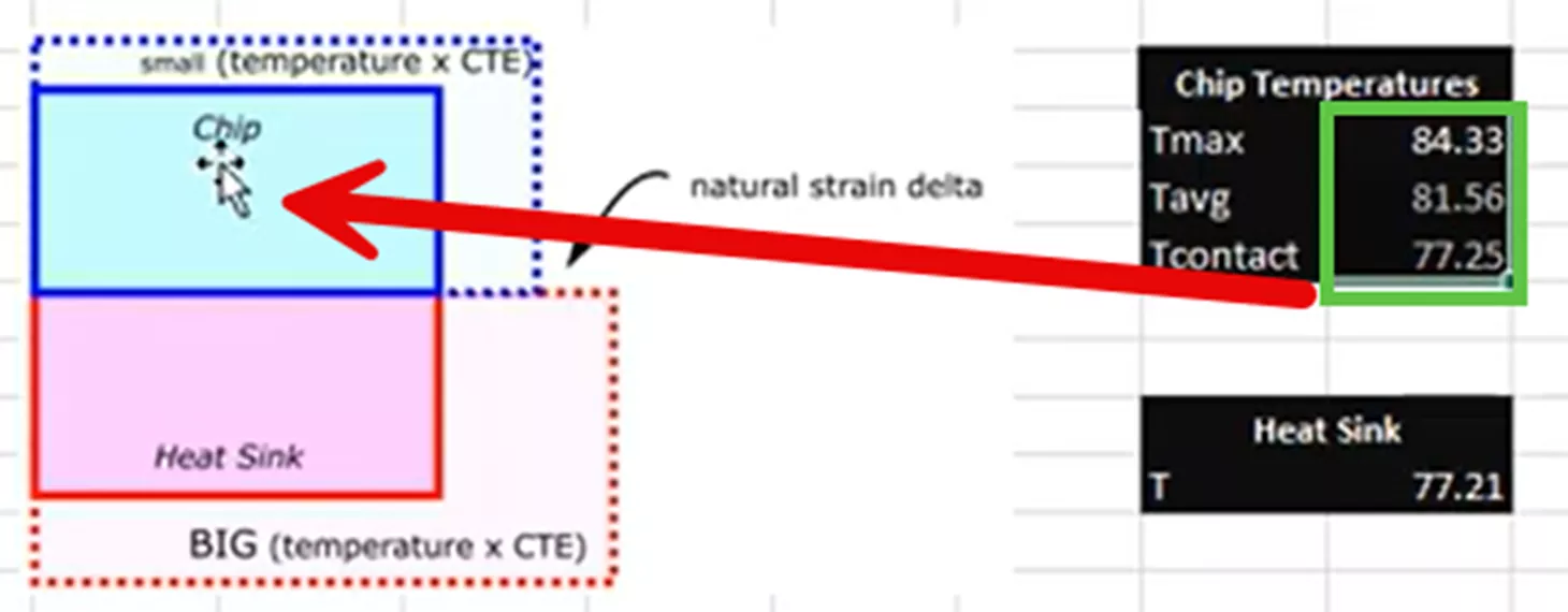
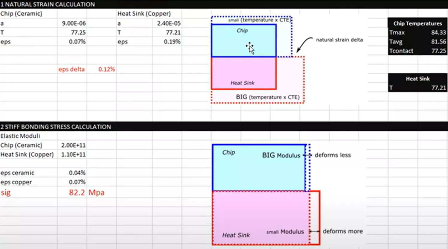
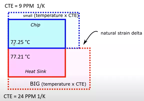
This calculation had several calculated temperatures for the chip (shown above in green) because it was hottest in the middle and cooler on the outside. Which temperature should be used to describe the chip in this structural hand calculation?
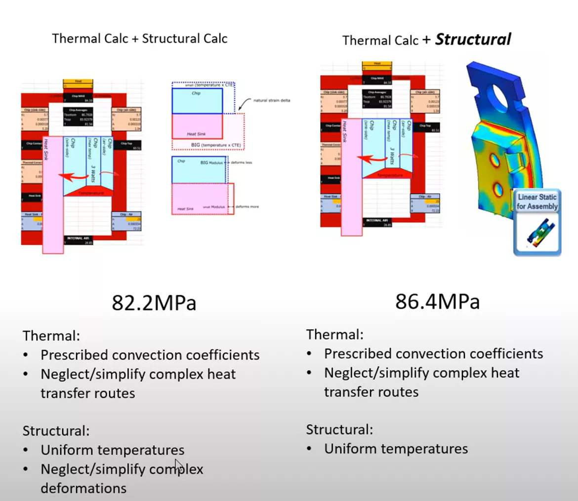
As a best practice, we are looking for the most conservative results possible. In this scenario, since the two components will be bonded, we want to calculate for the most thermal stress. This will happen when the chip expands the least amount possible and when the heat sink expands the most possible. This means that we will use the lowest temperature for the chip at 77.25°C and the largest temperature of the heat sink to simulate the most conservative scenario and result set possible.
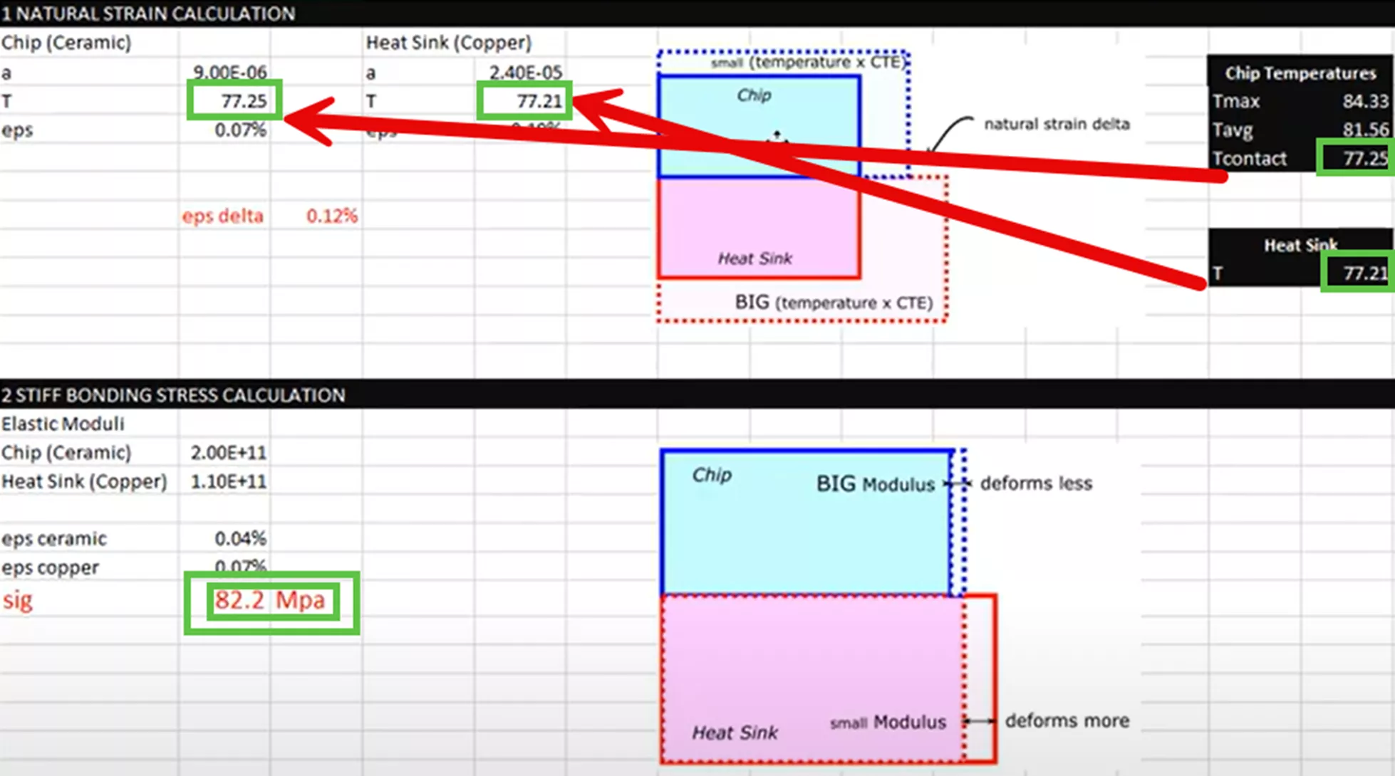
This provides a contact stress of 82.2 MPa.
To summarize, a lot of assumptions were made for both thermal and structural hand calculations to come up with a result.

The biggest assumptions were coming up with the convection coefficients and simplifying the complex heat transfer routes from the microchip to the PCB and heat sink, which were considered negligible in our calculation.
Method 2
Heat Transfer Calculations by Hand, Stress Calculations with SOLIDWORKS Simulation
Next, let's explore and improve our results by running the structural step of our workflow with SOLIDWORKS Simulation instead of hand calculations. We will use the static structural analysis tool that is part of SOLIDWORKS Simulation Standard licensing, as well as our temperature calculations from our previous hand calculations, so we know approximately what the temperature load will be.
Let’s open the model in SOLIDWORKS.
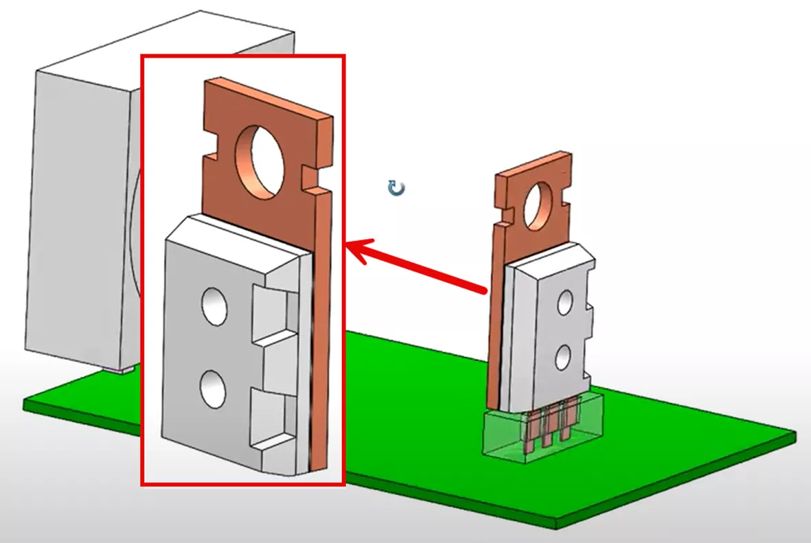
For this particular study, we don’t have temperature results on the PCB and connector geometry. Let's simplify the model to just the microchip geometry and the heatsink.
To begin, we'll create a static study in SOLIDWORKS and name it Standard Static..
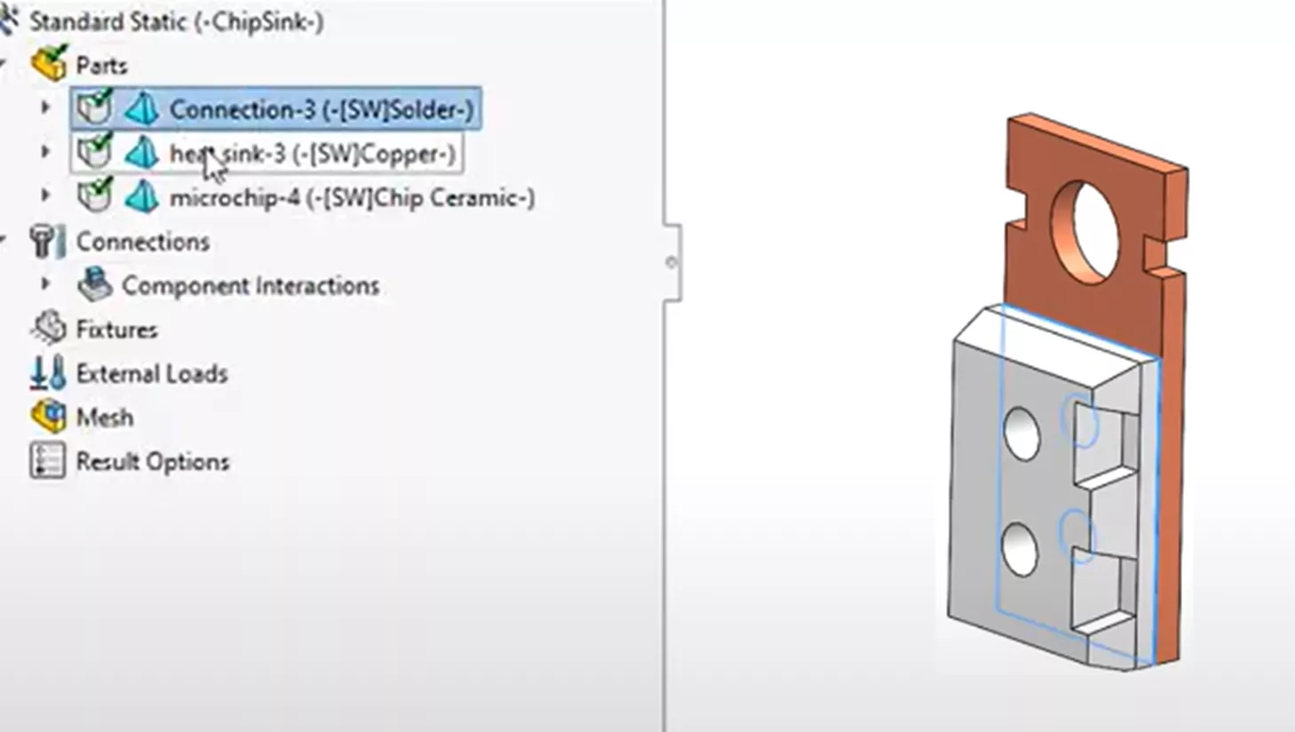
The materials have already been assigned to the geometry by the CAD model and brought over to the simulation study, where solder is defined on a thin geometry between the microchip and the heatsink. A copper material is assigned to the heatsink, and a ceramic material is assigned to the microchip.
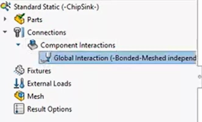
For geometry interactions, we are using the global interaction of bonded. This will assume all initially touching geometry is bonded.
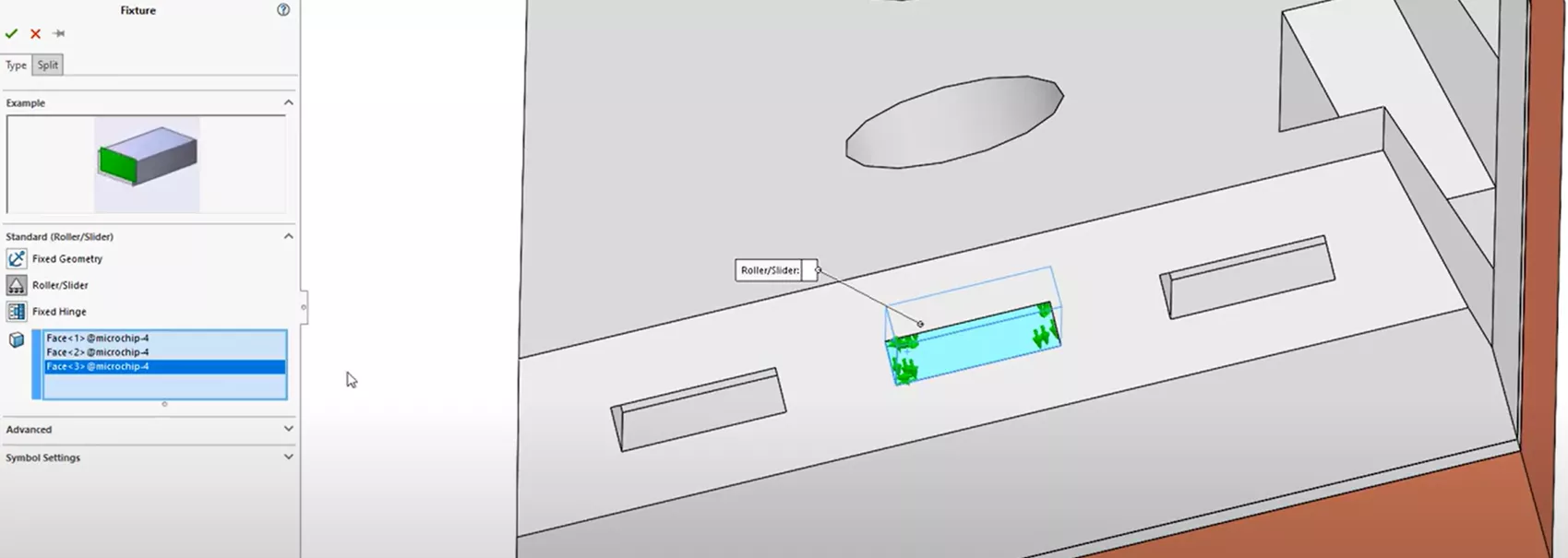
To fix and stabilize the model in 3D space, we will use Roller/Slider boundary conditions on the selected faces for now, but explore alternative boundary conditions later.
The next step is to apply a temperature load for the chip and heatsink components from our hand calculations. We will include the solder geometry as part of the chip as an assumption here.
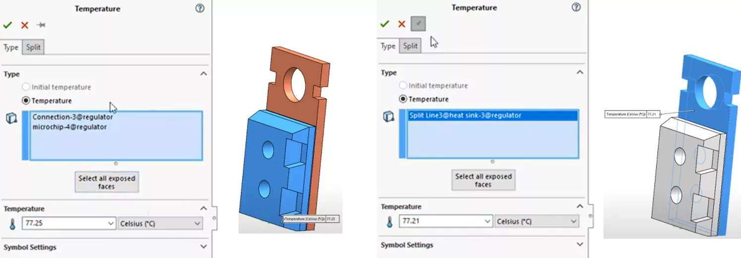
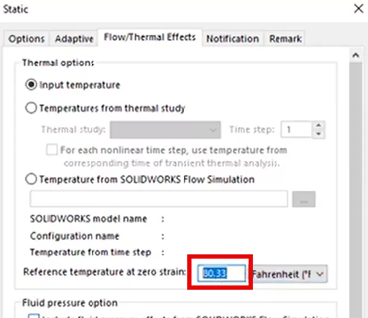
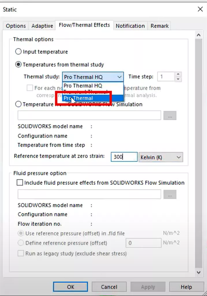
Now, in the study properties, we must assign the initial temperature of all matter (unless otherwise specified) in the analysis. In this case, it will be 300 K, or about 80.33°F. Click the Flow/Thermal Effects tab and enter this value under the option Reference temperature at zero strain.
Lastly, we will discretize the model with the Blended Curvature-based meshing strategy and run the simulation to see what kind of contacting thermal stresses develop.
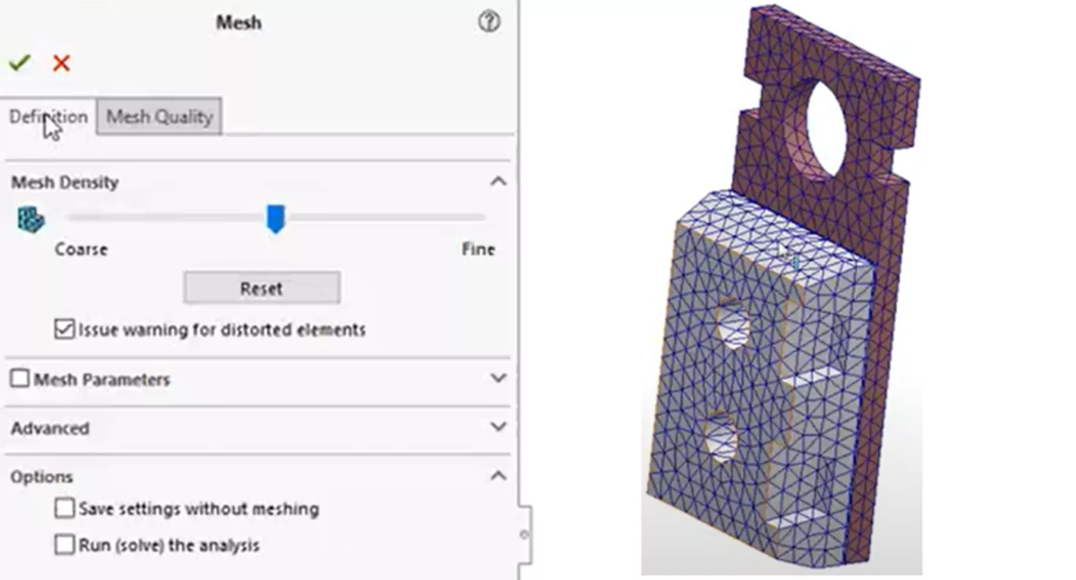
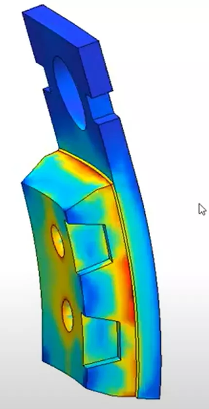
Looking at the stress results, the heatsink wants to expand more than the ceramic microchip, resulting in a stress development at the bonded region and a bending motion to the left.
If we measure the average stress at the contacting face of the microchip, the value is found to be 86.42 MPa (shown below).
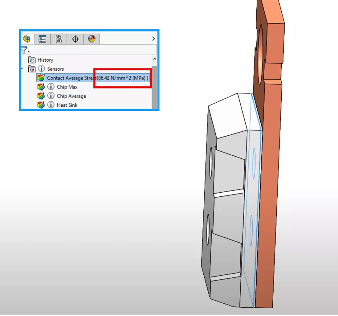
Very comparable to the 82.2 MPa value determined by hand calculations, but now we are considering the more exact shape of the geometries and their responses, where before we were making larger assumptions.
Method 3
Running Both Steps with SOLIDWORKS Simulation
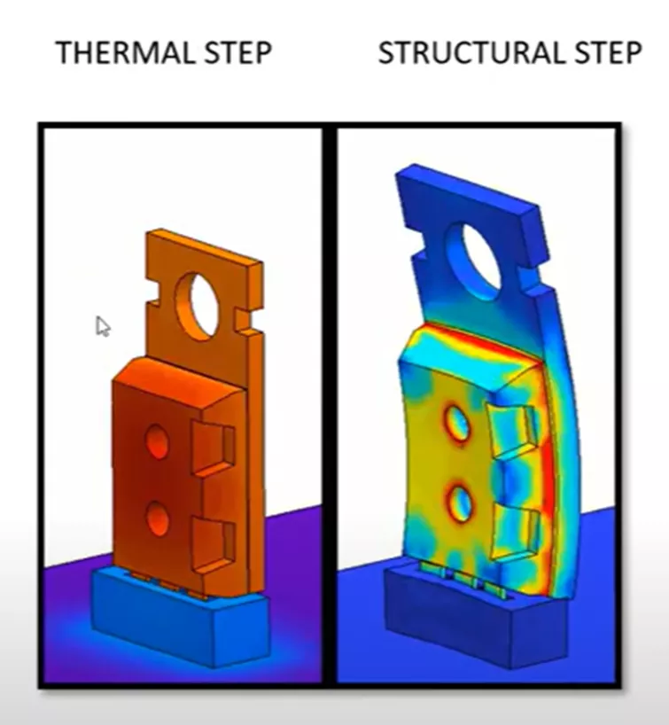
Next, we will forgo the hand calculations altogether and use SOLIDWORKS Simulation Professional to determine the initial temperature distribution using a thermal study. This will allow us to be more specific with our geometry regarding the heat transfer, and we can account for non-uniform temperature gradients. The same structural step will be performed as before, but will include additional details from the connector geometry, as shown below.
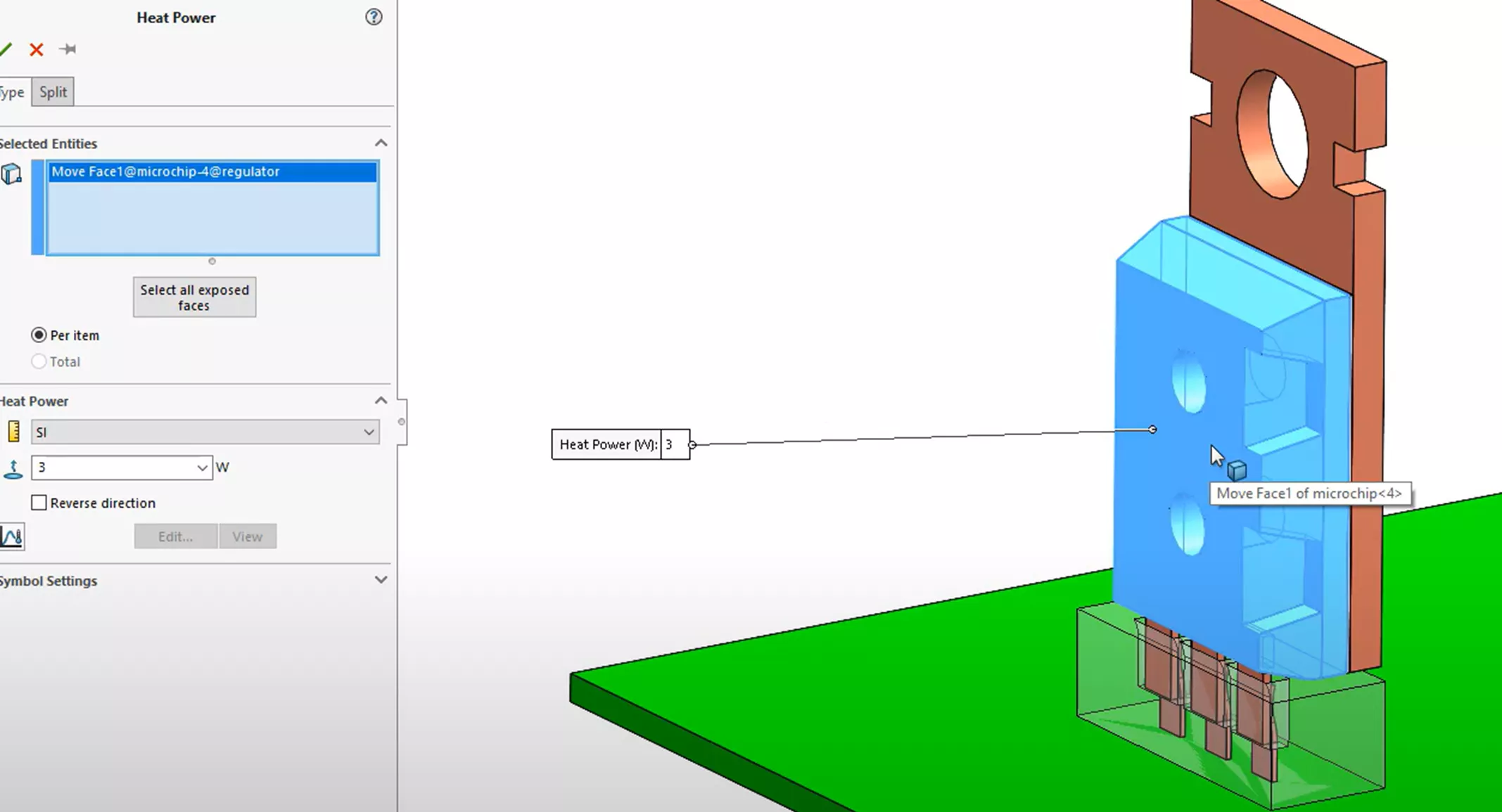
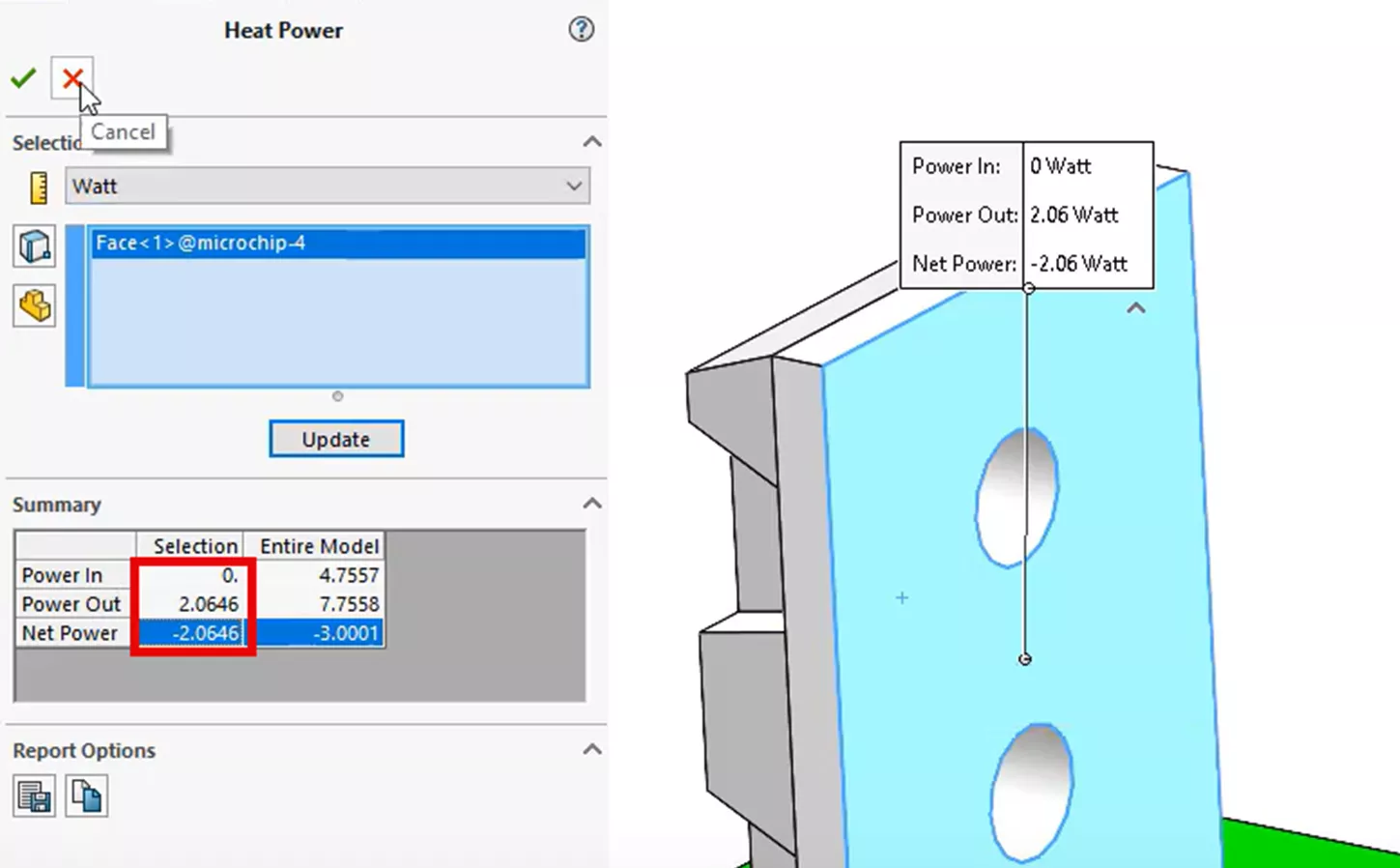
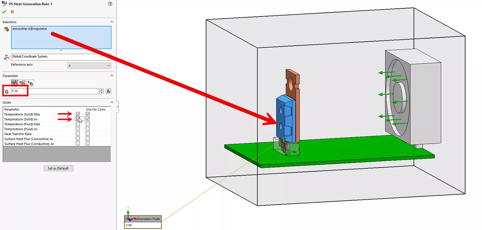
Here, a thermal study was created with SOLIDWORKS Simulation Professional. Let's begin the thermal step setup by specifying the heat source of our simulation with a Heat Power feature.
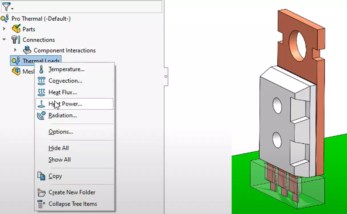
We'll grab the full body of the microchip and apply a 3-watt heat source.
Now that heat has a way into the system, we need to determine how it will leave the system - through convection. We will apply a primary convection feature to all exposed surfaces of the heatsink and the bottom connector geometry. To best represent the heat transfer to the surrounding air, we will add a convection coefficient of 50 units, maintaining consistency with our hand calculations. This is a significant assumption we are making. As noted in the initial hand calculations, the resulting temperatures can vary dramatically when the convection coefficient value is changed. Finally, we will set a bulk ambient temperature of 300K, as we assumed in our hand calculations.
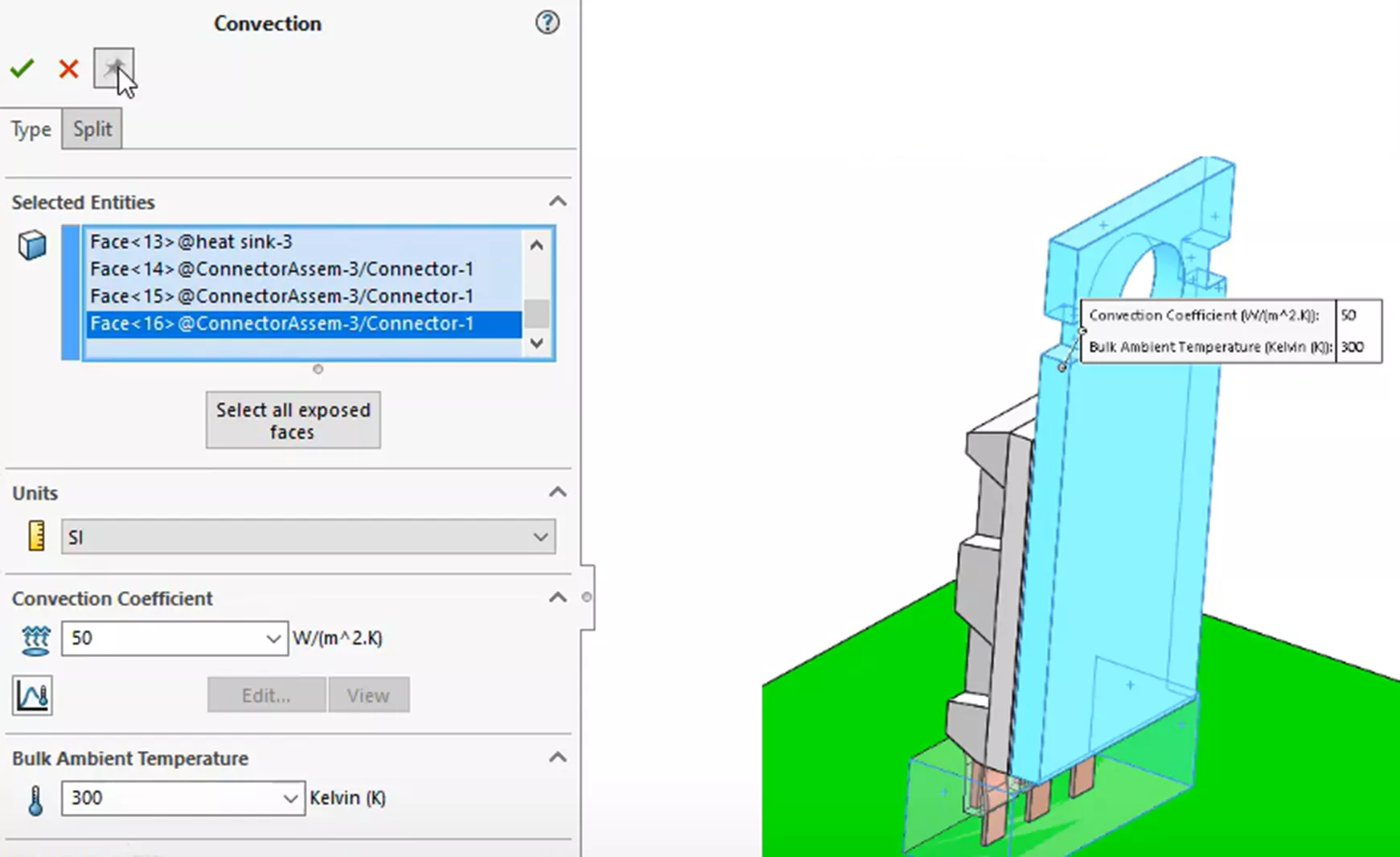
An additional or secondary convection coefficient feature will be added to the exposed faces of the microchip. To remain consistent with our hand calculations, this coefficient will have a much lower value of 25 units, as much less heat transfer occurs from the ceramic material.
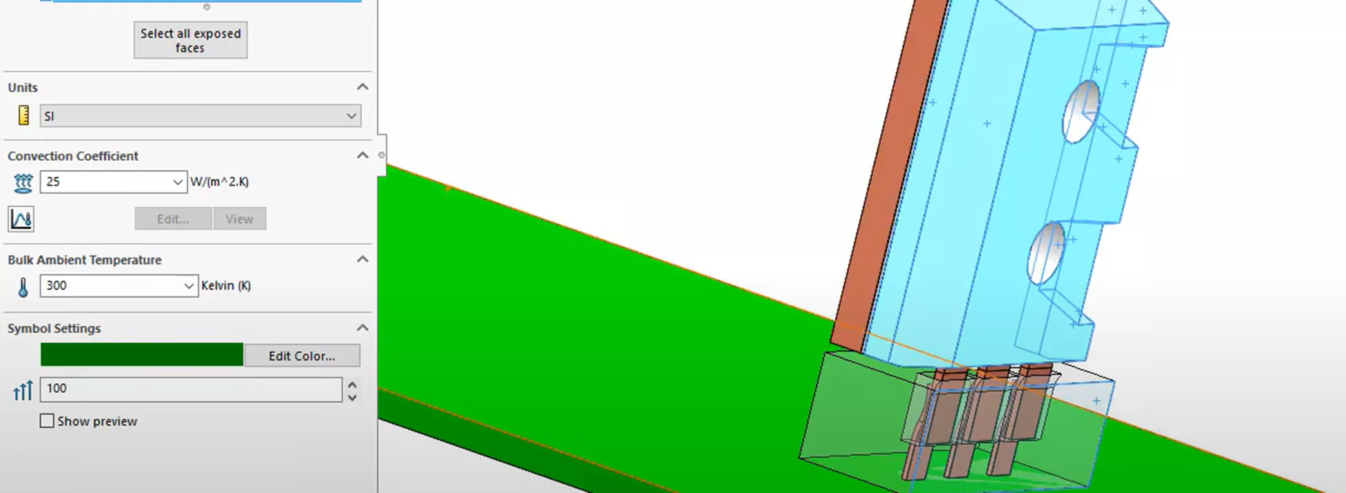
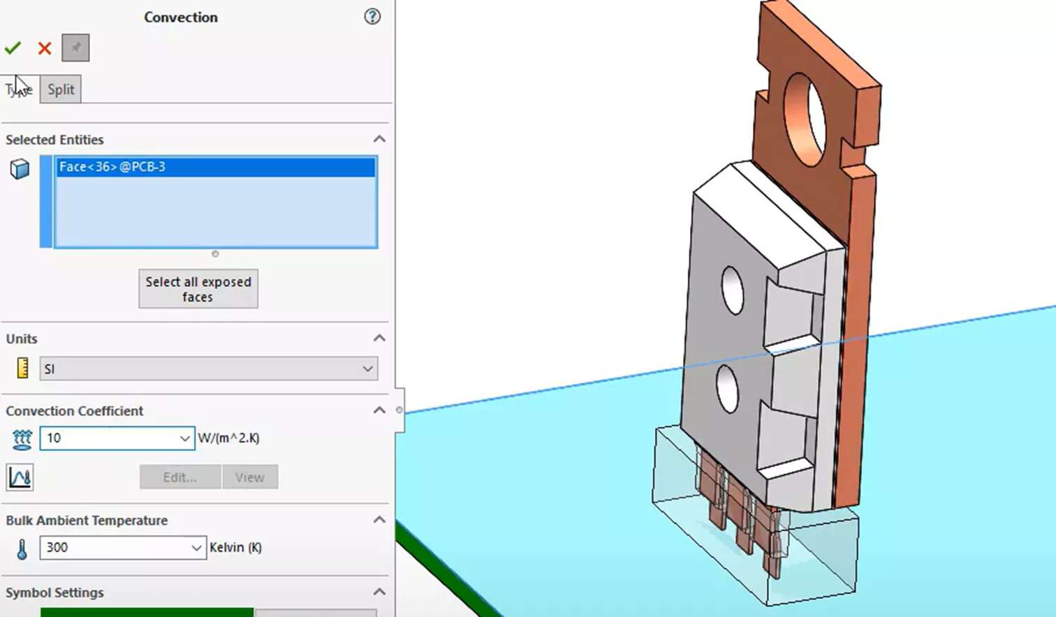
Finally, we will add a third coefficient feature to the surface of the PCB with a convention of 10 units.
So that takes care of the cooling aspect of the heat transfer. Now, to address how the heat transfer travels through the various components.
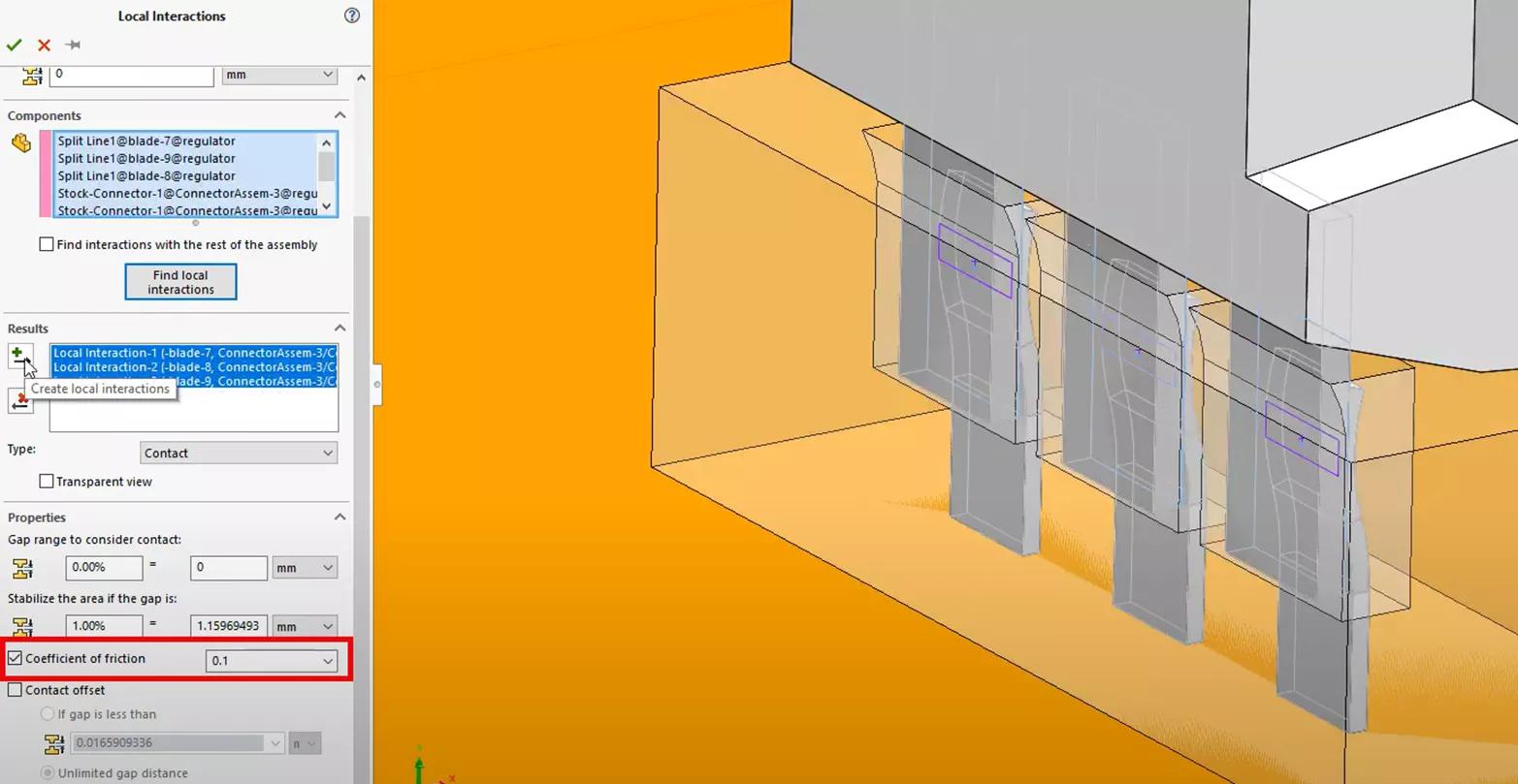
Let's start by selecting all the components that make up the microchip, thermal compound, heatsink, and copper connectors, and apply a component-level interaction feature to those components.
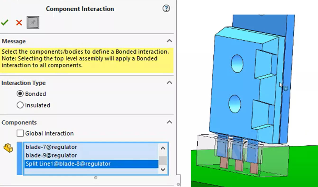
Then, we will apply a second component-level interaction feature to the PCB, the connector, and the three leads shown below. These will be considered bonded to each other.
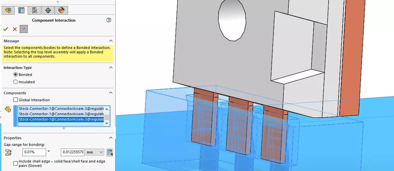
However, if we zoom into the copper connectors of the microchip and the contacting leads of the connector, those interactions have a spring-like quality and are much different compared to the other interactions. They will have a resistance associated with them due to the rough connection between connector components. We will apply a separate and local interaction to the contacting region to account for the additional thermal resistance.
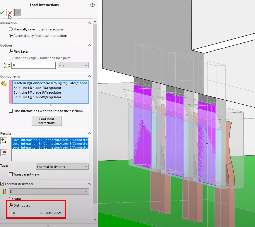
A local interaction feature is created, and we detect and select the contacting faces between the leads and the copper connectors. A distributed thermal resistance of 0.01 (Km2)W is added.
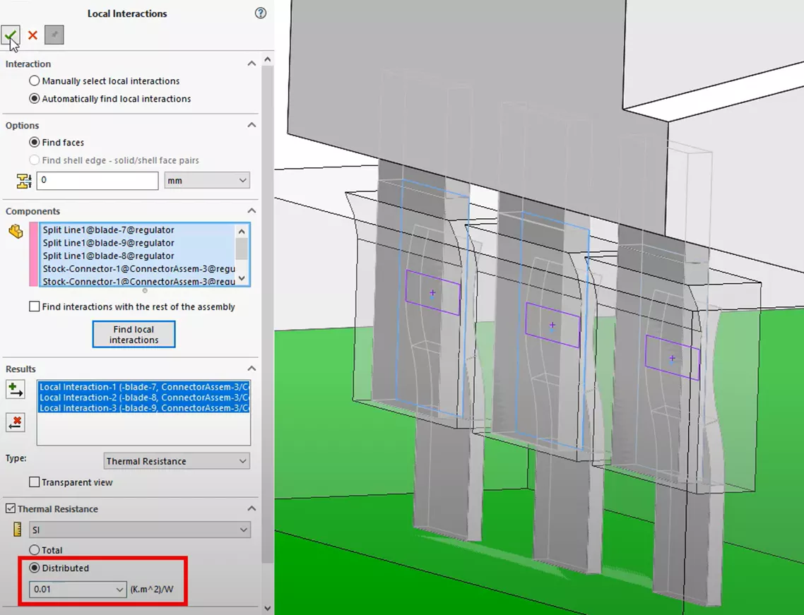
A similar thermal local resistance interaction feature will also be added between the microchip connectors and the connector body housing.
This last feature finishes the setup of the thermal study. We will mesh the model using the same mesh settings as before and run the study.
Looking at a temperature plot, we can see a maximum calculated temperature of 82.33°C as well as the temperature gradient for the entire model.
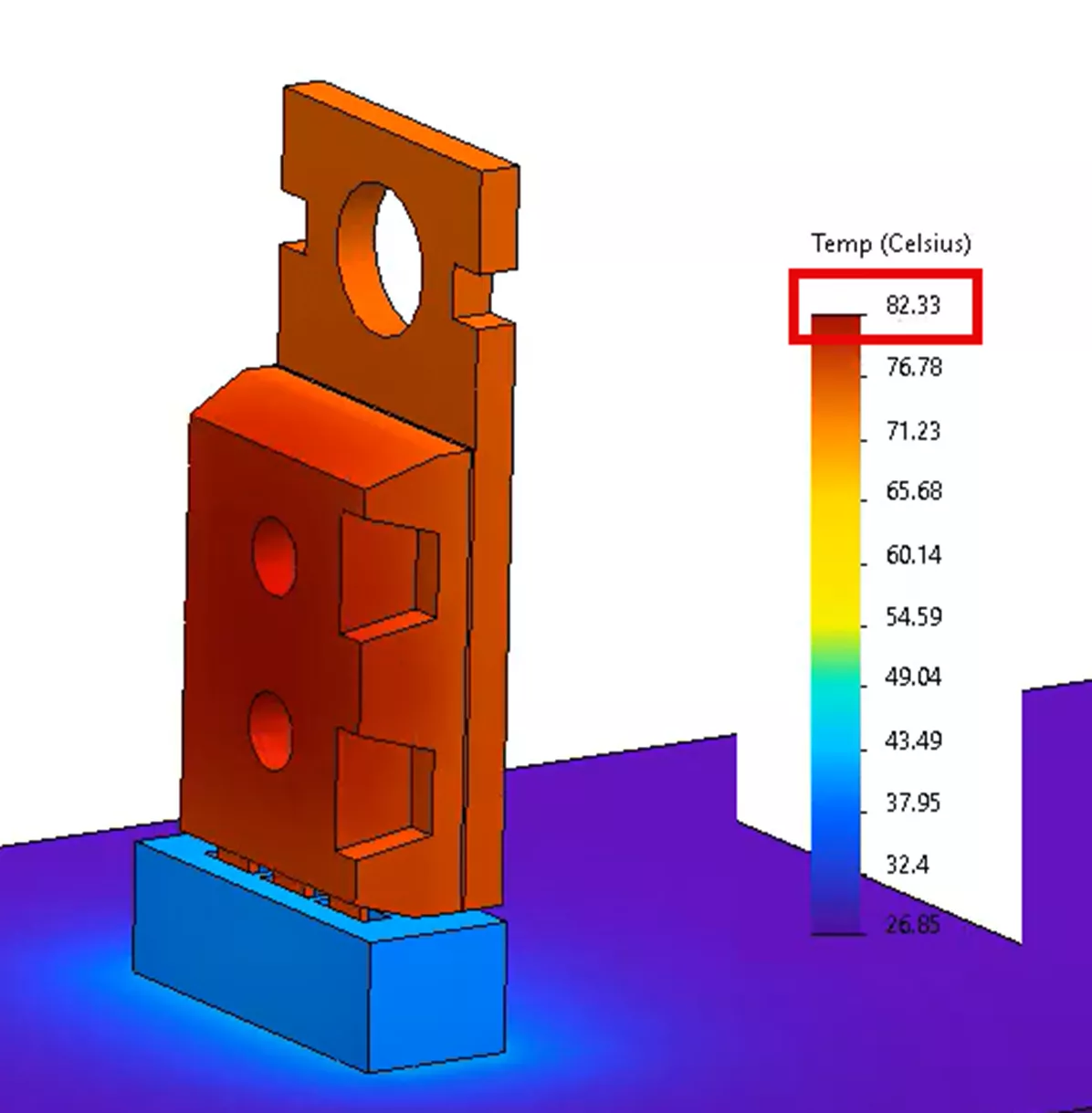
We’ll take these temperature results and bring them into a structural study to obtain our thermal stress. But before we do that, since we ran this thermal study, we can examine the calculated heat transfer from the microchip to the heat sink. Before, we had hand-calculated that value to be about 2.2W. If we use our post-processing tool List Heat Power, we can see that the actual heat transfer is closer to 2.06W.
Another static study is created in the same exact way we did for method 2 of this article. Since we’ve included more geometry, we can add more detail to the setup by introducing friction to our interactions among the connectors.
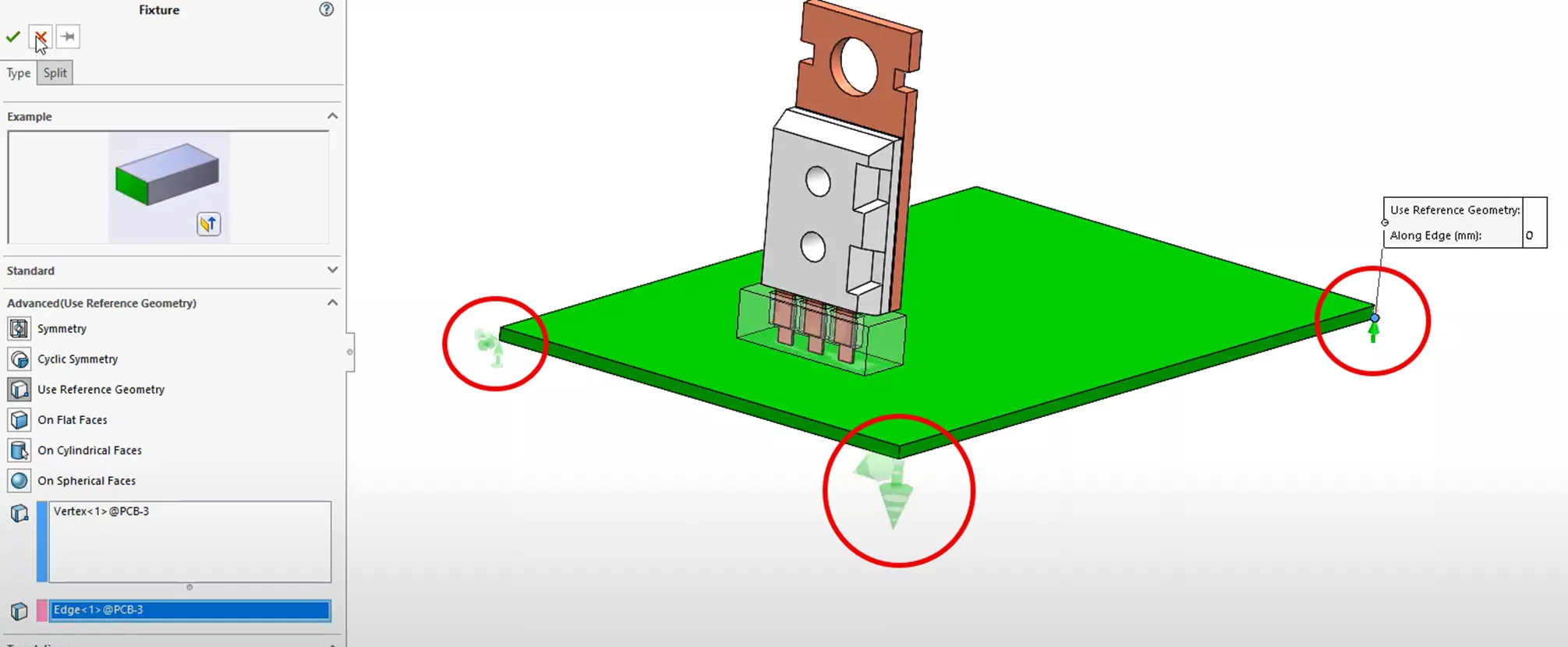
In the previous structural study, we simplified the fixture. Now, since the PCB is being included, we will apply three fixture features to reduce the degrees of freedom so that the PCB will be stable for the calculation and be able to deform.
Now, we can import the thermal load from the thermal study by selecting Thermal Effects from the External Loads folder in the Simulation Design Tree.
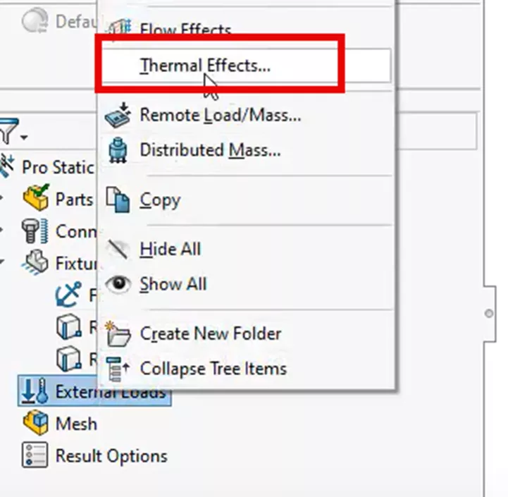
In the Study Properties pop-up window, click the radio button for Temperatures from thermal study and select the Pro Thermal study from the pulldown menu. Click the OK button to accept the application of the thermal results to this structural study.
We meshed the model with the same curvature-based mesh settings and ran the study.
Looking at a stress result plot with imported temperatures, a very similar stress gradient can be seen in our stress plot.
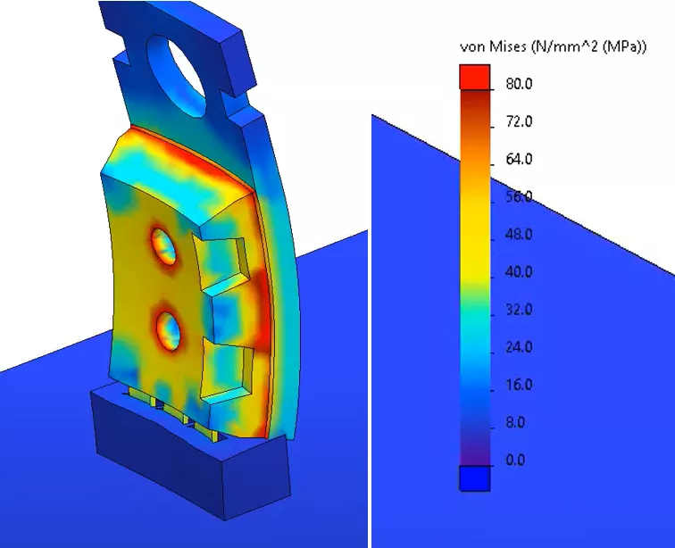
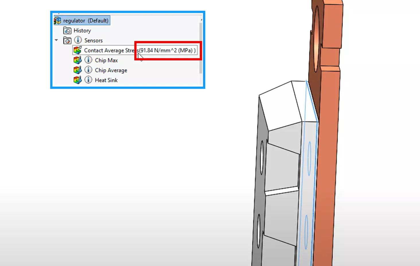
When we interrogate the same contacting face of the microchip as in our previous structural study, we see that the average stress result has gone up to 91.84 MPa.
This is a more accurate result set, as we are making even fewer assumptions than we did in the first two approaches. With this latest approach, we are no longer assuming uniform temperatures for our thermal model. We can develop a higher more realistic internal temperature for the microchip with a calculated temperature gradient that lessens as we move away from the centroid of the microchip.
Secondarily, we can calculate more complex heat transfer pathways by using the exact geometry versus simplified hand calculations, resulting in a more accurate heat flux. We are also modeling the thermal resistances introduced in the thermal study. These measures are all causing additional stress at the contacting region.
Method 4
Running the Heat Transfer with SOLIDWORKS Flow Simulation & the Structural Analysis with SOLIDWORKS Simulation
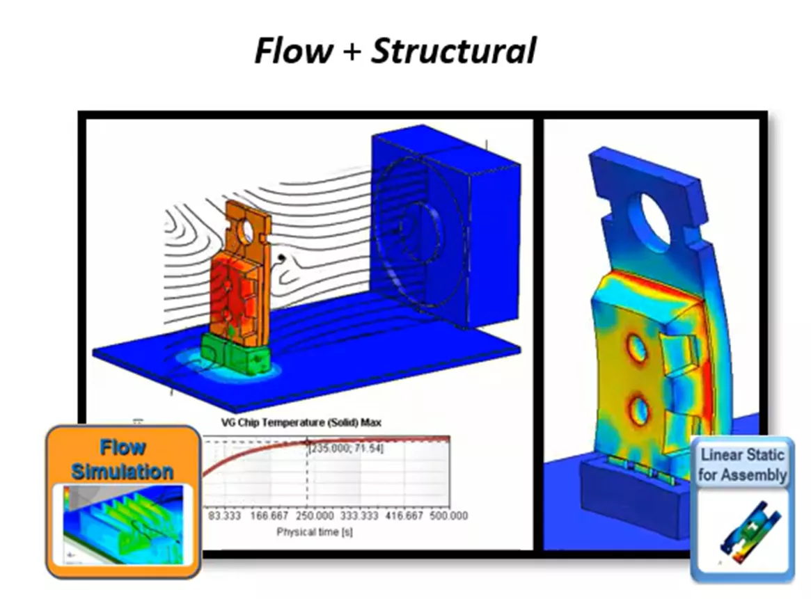
Lastly, we will incorporate the use of SOLIDWORKS Flow Simulation for our heat transfer step. This will automatically calculate the convection coefficients, so we don’t have to guess at them for our thermal step.
SOLIDWORKS Flow Simulation specializes in simulating fluid dynamics and heat transfer, so we can consider many more aspects of the thermal system. This section will introduce the workflow for SOLIDWORKS Flow Simulation and show how to inject these more detailed results into SOLIDWORKS Simulation for our structural step.
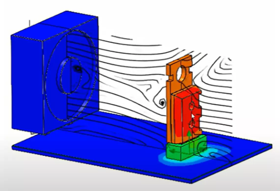
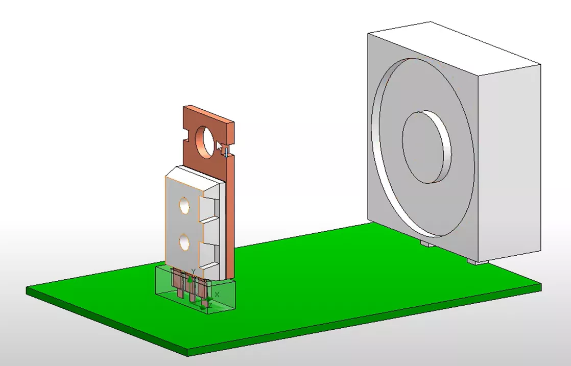
Below, we have extended our thermal model to include a fan. The fan will be pushing the air over the thermal model, so we can now consider forced convection over the microchip for our thermal step.
We will create a new external SOLIDWORKS Flow Simulation Project with the conduction physical feature turned on, and air as the default fluid medium.
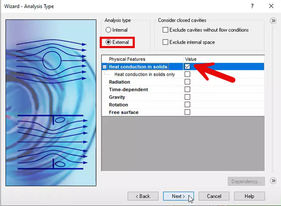
“Insulator” will be chosen as the default material in the wizard as a temporary measure, as we will override our material definitions by selecting them locally later in the workflow.
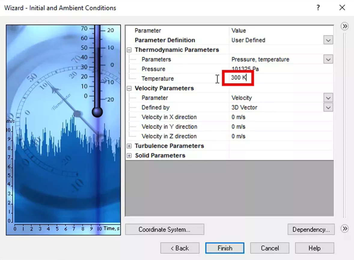
In the last section of the wizard, an initial temperature will be entered under the initial and ambient conditions section. To be able to keep with our previous comparisons, 300 K was entered since that is what we used for our initial hand calculations. The new project was created by finishing the wizard.
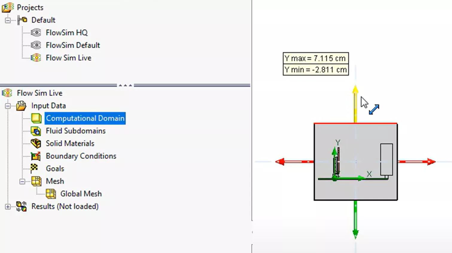
We can see our new project created below with the feature tree to the left. In this new project, we reduced the volume of the computational domain. The computational domain is the volume of space that our flow project will simulate our fluid dynamics and thermal model step.
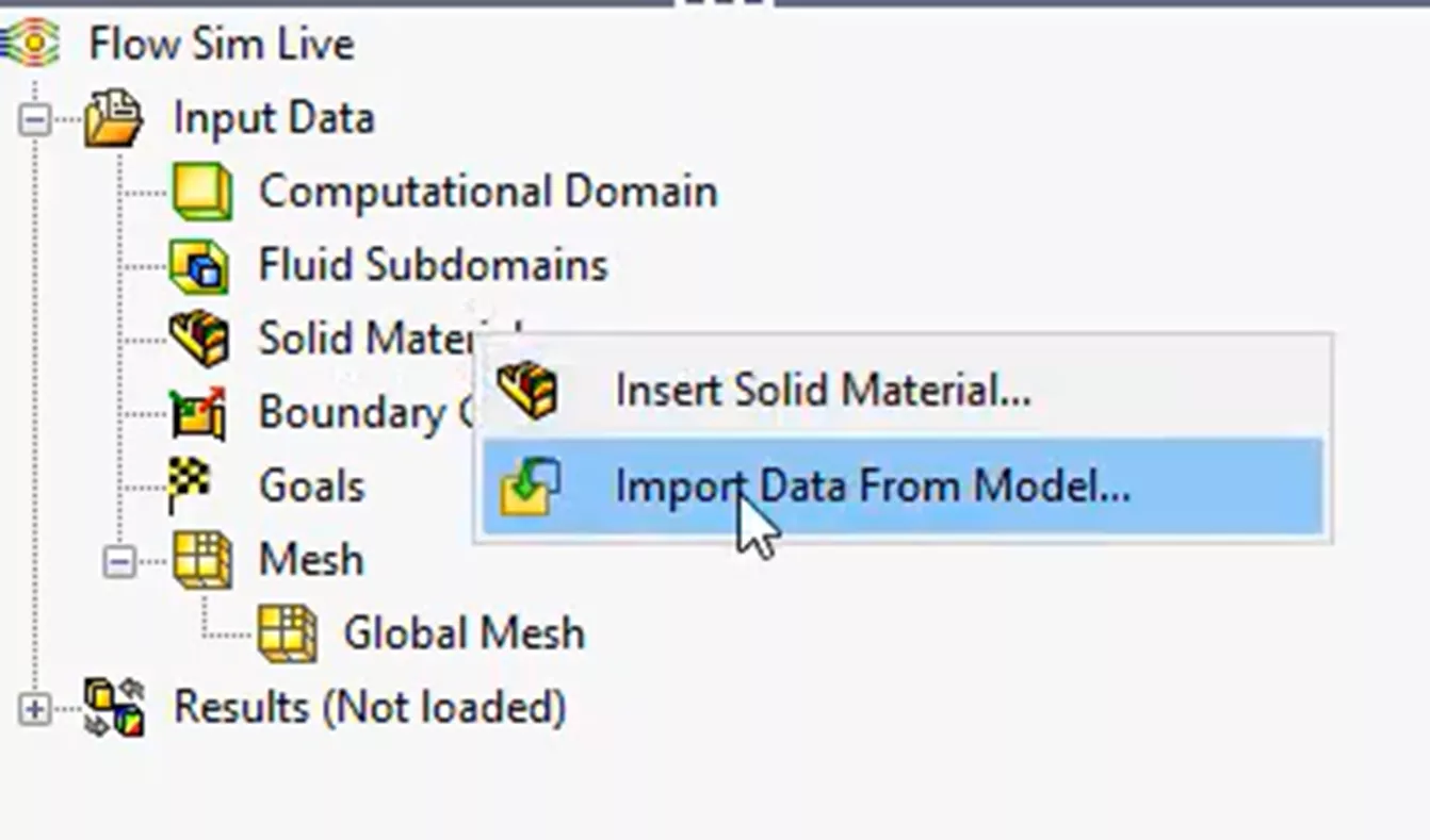
Next, we will import our material properties from the CAD model directly. This will allow us to be consistent with our materials among all of our previous simulations so far.
Afterward, we will assign a fan feature to the existing face of the fan component on the model.
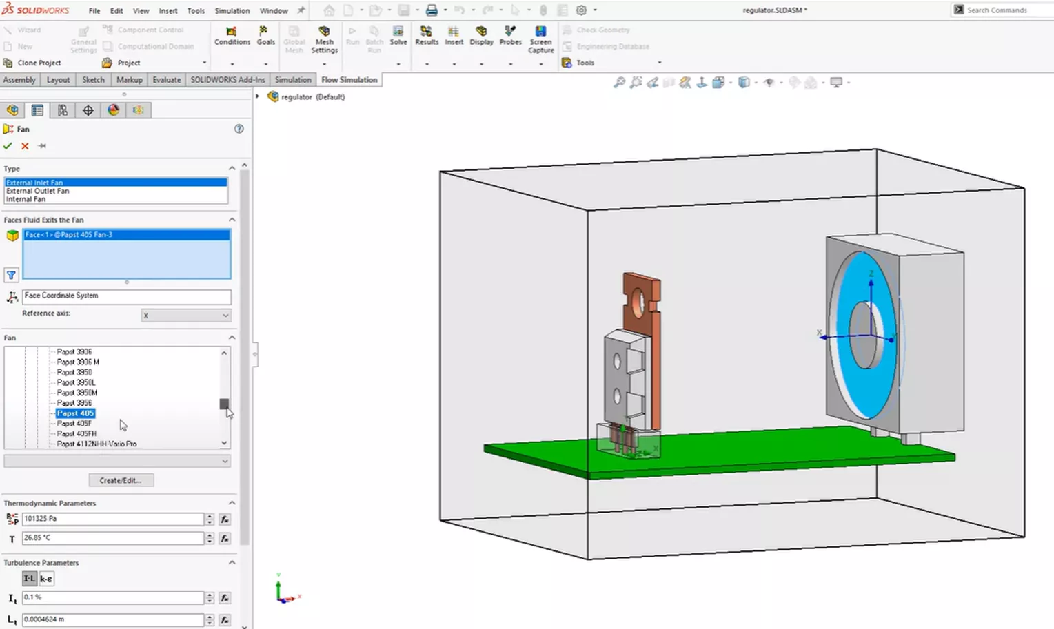
This allows us to simulate or idealize the air fluid medium’s response with a specific fan without having to include the actual blades and the movement of the fan. Including the blades and the movement would greatly increase our computational resources and calculation time in our project.
Next, we will introduce a similar volume heat source of 3 watts to our microchip component, just like in the previous thermal steps with SOLIDWORKS Simulation FEA.
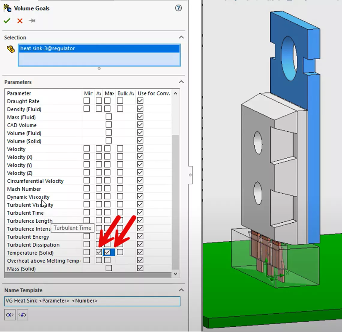
Further down in the PropertyManager on the image above, we will also include two Engineering volume goals to track the maximum and average temperatures of the microchip.
Engineering goals are a way to keep track of important values and monitor important aspects of your project in general. It is also a way to ensure that your SOLIDWORKS Flow Simulation solver can calculate results that are as accurate as possible by choosing what result parameters are important.
We will apply some contact resistance on the same contacting faces on the copper connectors of the microchip and the contacting leads of the connector, as in the FEA thermal study.
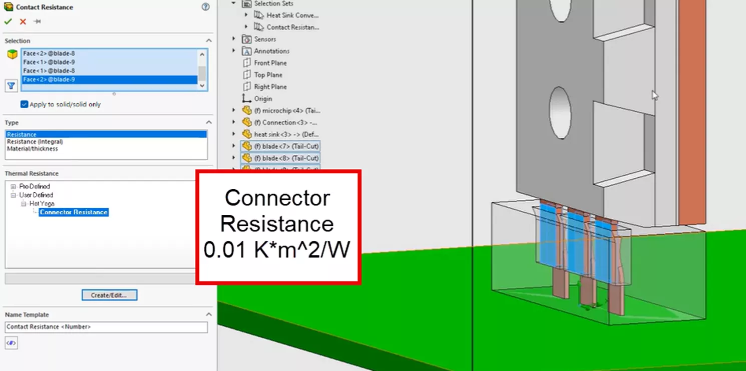
As a reminder, we selected these contacting faces, as they have a spring-like quality and are much different compared to the other interactions. They will have a unique resistance associated with them due to the rough connection between connector components.
Next, we will add a few more engineering goals.
We will add goals for tracking the maximum and average temperature of the heatsink.
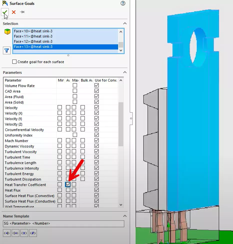
We will also add these heat transfer coefficient surface goals below to compare the calculated heat transfer coefficients to the estimated coefficients used in our previous thermal simulations.
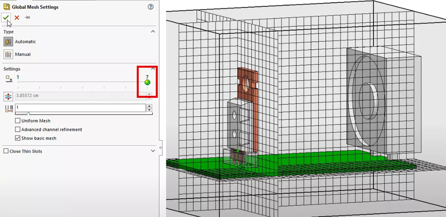
All that remains is to discretize or mesh the model. We will refine the mesh by first increasing the level of initial mesh to 7. This will give us the starting or maximum mesh detail (shown below).
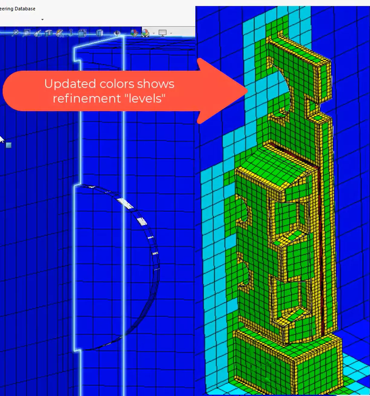
Next, we will apply some local mesh refinement around the components that make up the microchip geometry using the highlighted settings.
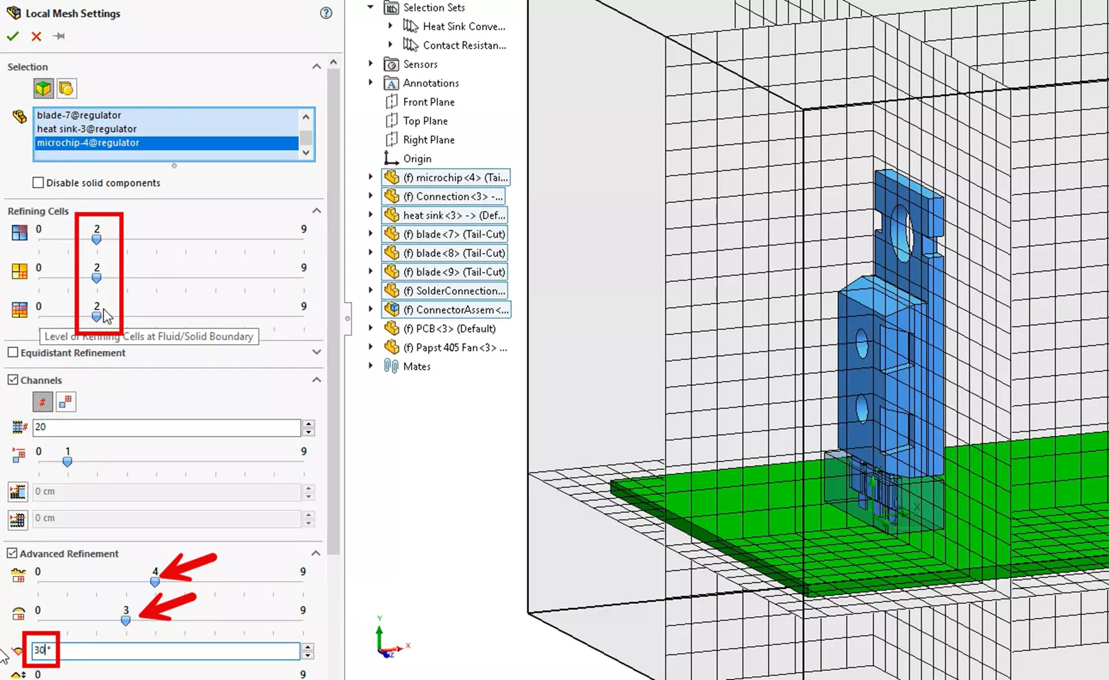
This yielded a much more detailed mesh surrounding the microchip geometry.
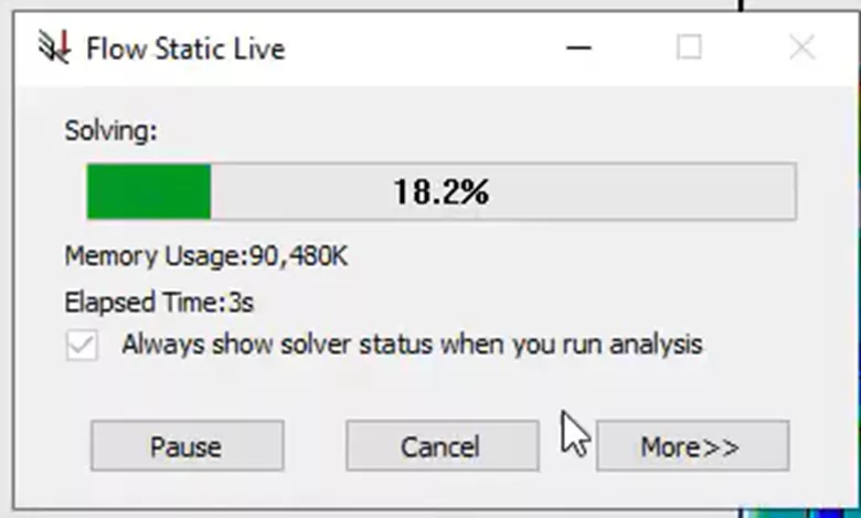
We run the SOLIDWORKS Flow Simulation project, and during calculation, we can monitor our solution with the solver window shown below. CFD simulations take much longer to run than most FEA studies. This allows us to observe, in real time, the development of the result parameters both qualitatively and quantitatively. The benefit of the solver window is that we can observe the development of the result set. If things don’t look as anticipated, we can always stop the calculation early and troubleshoot our project.
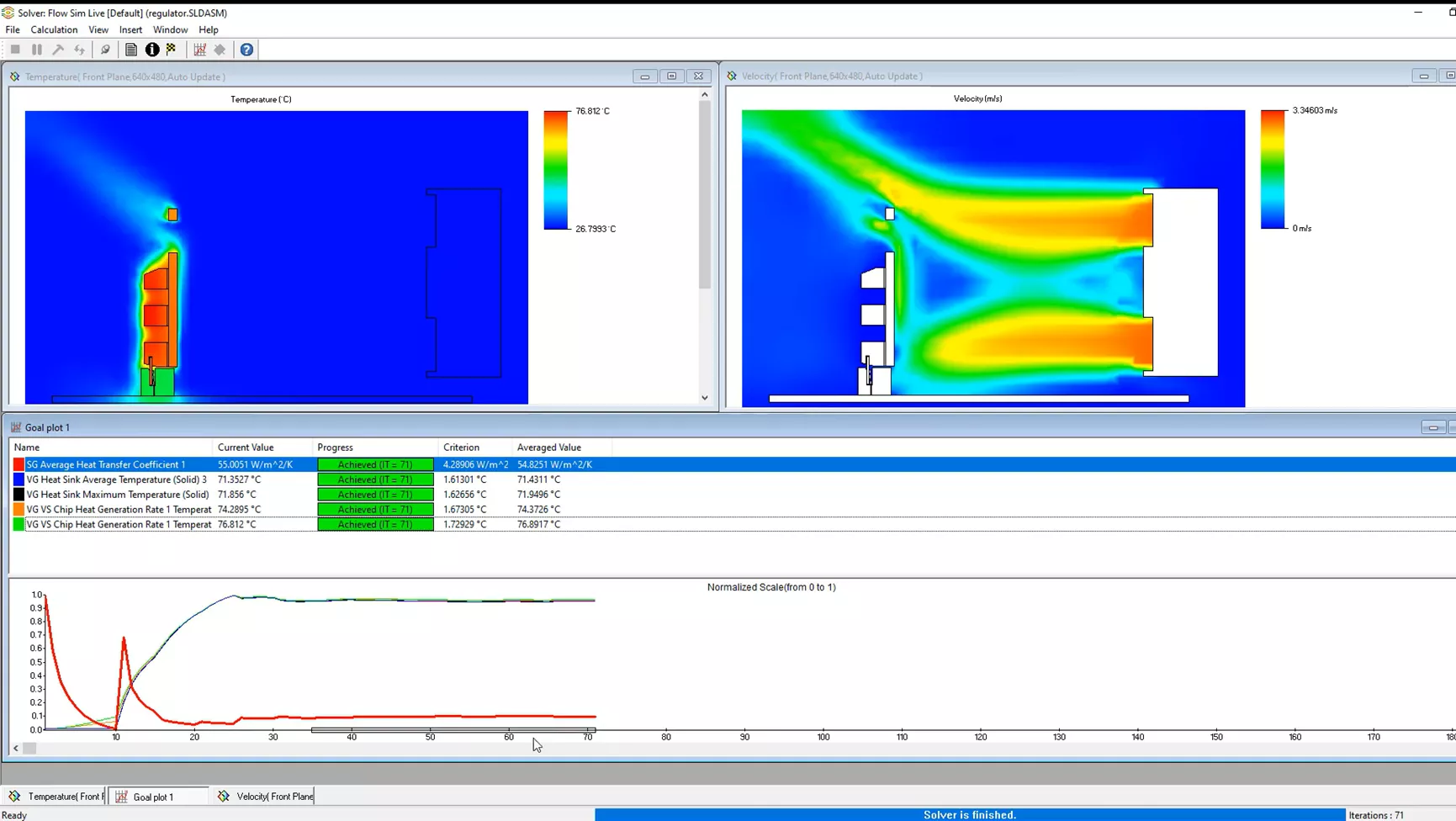
Running the thermal step in SOLIDWORKS Flow Simulation gave us the following results (shown below). First, our maximum temperature for the microchip geometry is about 76-77°C. This is a few degrees cooler than our previous SOLIDWORKS Simulation Professional thermal study.
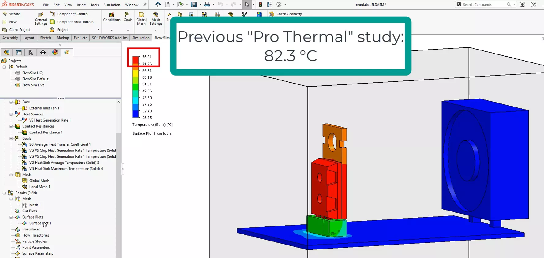
Recall that this result set considers the development and calculation of all the heat transfer coefficients in the system and is considered the more accurate result set.
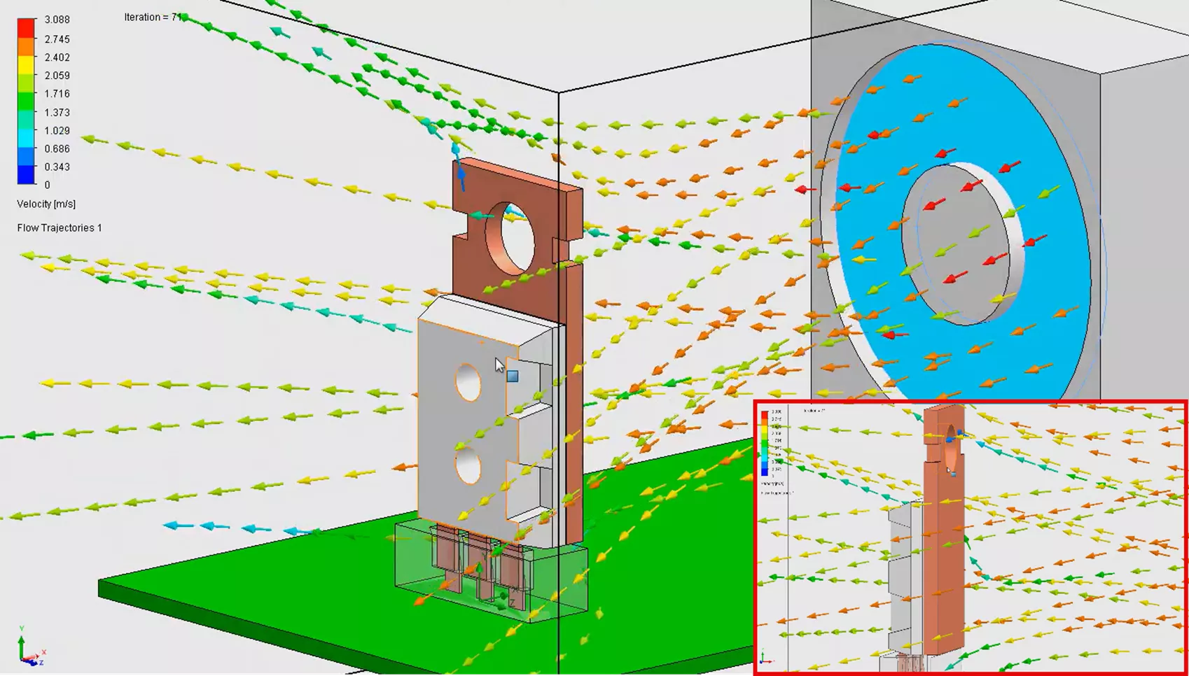
Next, we can observe the flow trajectories result plot. We can directly observe and animate the behavior of our flow fields with any supported result parameter. Below showcases the velocity of the air fluid medium traveling over the microchip. The animation aspect of this plot really allows you to observe and gain insight into how the system responds.
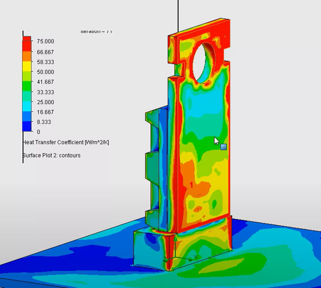
Lastly, we will create a heat transfer coefficient surface plot so we can see calculated distribution of these results. Previously, with SOLIDWORKS Simulation Professional, we were at most only able to estimate and apply the same uniform coefficient value on full faces of our study.
Now with SOLIDWORKS Flow Simulation, we can calculate and develop more realistic heat transfer coefficient gradients that are nonuniform throughout all the faces in the system, which is what we observe in real-world results.
Now that we have our thermal results from our updated thermal step, we will import these results over to SOLIDWORKS Simulation FEA just as before.
We will create a third study for our structural step in the exact way as the previous FEA methods. You could even copy the study to prevent human error. We will import our thermal results in the study properties of the study from our CFD project as shown below.
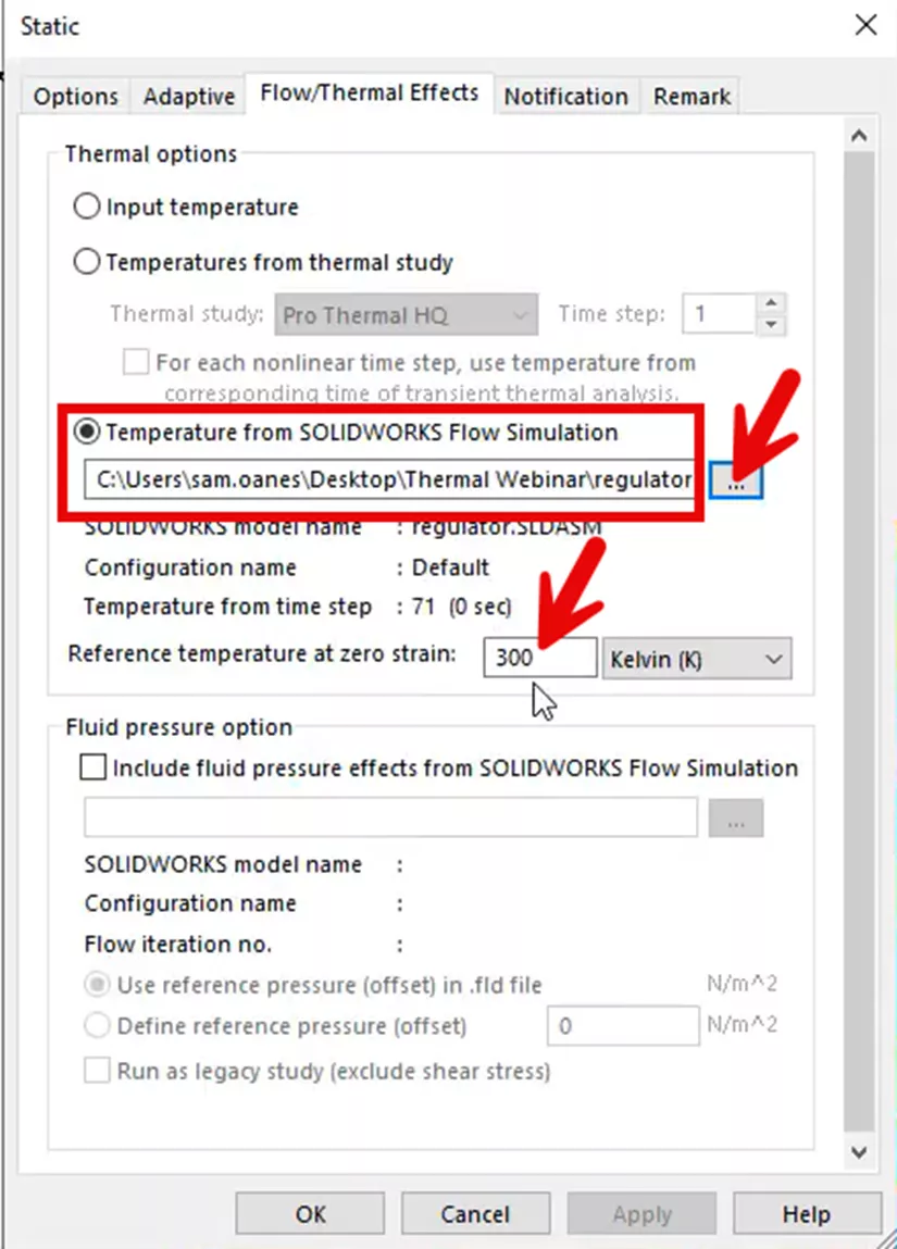
We also specify the reference temperature at zero strain to be the same 300 Kelvin as in our hand calculations and other previous studies.
Now we are ready to run the final structural step with our CFD thermal results.
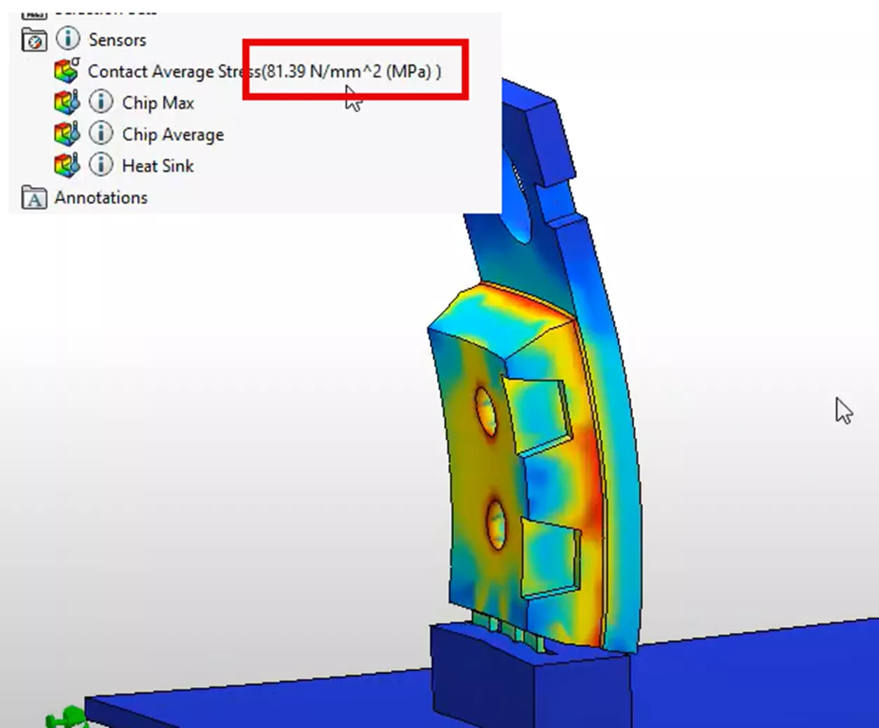
Looking at the same sensor plot analyzing our contacting stress, we can see that the stress result is lower than the previous iteration at 81.39 MPa.
This last result represents the scenario where we have the least number of assumptions regarding thermal and structural steps. More specifically, we are no longer estimating convection coefficients of heat transfer, and we are dealing with more complex and non-uniform thermal loading as well.
Final Thoughts
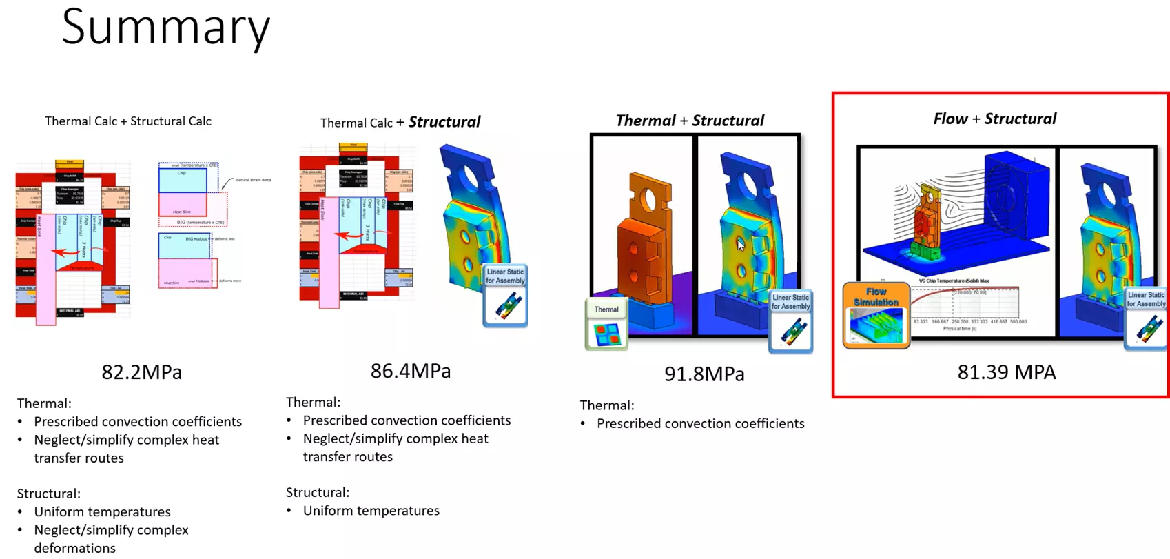
We reviewed the usage of quite a few methods for conducting the same analysis, mixing software tools and hand calculations.
In method 1, we used hand calculations for both the thermal and structural steps. In method 2, we kept the hand calculation for the thermal step and used FEA for the structural step. For method 3, we used FEA for both the thermal step and the structural step. Lastly, for method 4, we used CFD for the thermal step and FEA for the structural step.
In conclusion, the use of SOLIDWORKS Simulation enables more precise representation of system geometries and reduces the need for assumptions in defining boundary conditions. This leads to more reliable results when evaluating whether a design meets or fails to meet its performance targets.
Related Articles
SOLIDWORKS Flow Simulation 2026 - What's New
When to Move from Linear to Nonlinear Finite Element Analysis
SOLIDWORKS Flow Simulation Pickup Truck Tailgate Drag Analysis
SOLIDWORKS Flow Simulation Semi-Truck Drafting and Drag Impacts

About Enrique Garcia
Enrique has been involved in technical training since 2007 with SOLIDWORKS and Simulation tools and currently specializes in Simulation Products. He is a CSWE and was given Elite Application Engineer status at SOLIDWORKS world in 2018. Enrique holds a Bachelor's Degree in Biomedical Engineering from Arizona State University. He has worked alongside and learned from companies in the medical device industry developing orthodontic devices that specializes in the rehabilitation needs of many types of patients.
Get our wide array of technical resources delivered right to your inbox.
Unsubscribe at any time.